 RF cat corner
Grounding II – a matter of return conductors.
Nov 13, 2026Most misconceptions about grounding occur due to the lack of a clear idea of what a ground is and what it should do.
The goal of a ground is to provide to each signal conductor a reference conductor, allowing to contain the electromagnetic wave, to provide a shielding effect, even if sometimes very cruse, and to ensure proper flow of the return currents. These three functions are not independent.
Most EMC design rules are a consequence of this, as can be shown by a review of various ways to provide a ground, followed by an analysis of the ensued design rules.
The ideal: coaxial cables everywhere
Lab benches
The ideal would be to use coaxial cables for each signal. While it seems to be very cumbersome, this situation is actually very common in lab benches, comprising several metallic boxes connected by coaxial cables. A minima they are used for RF. Serious setups also use them for lower frequency signals. Very serious setups also use them for supplies, typically by using banana to coax adapter straight at the supplies output. High end setups use source measurement units (SMUs) directly fitted with coaxial cables.
In such a setup, the grounding is made by the boxes themselved and by the shields of the coaxial cables.
Nuvotronics coax
In addition to the wide scale of the labs, there are also very expensive ways, using modern 3D techniques, to manufacture coaxial cables on a micro scale. In applications where the costs can be afforded, this works definitely very well.
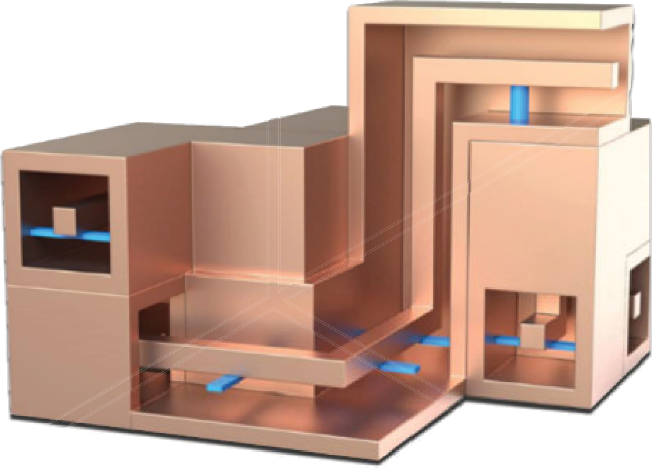 Copyright Cubic Nuvotronics, https://www.cubic.com/sites/default/files/2024-05/2023%20Nuvo%20Product%20brochure_R32_PRINT.pdf
Various real-world approximations of coaxial cables
The microstrip line
While microstrip lines never achieve the excellent shielding effect of coaxial cables, they are often good enough. While in coaxial lines, the signal line is tightly coupled to a fully surrounding shield, in microstrip line, this tight coupling is ensured by a close ground plane, which provides something like a proximity shielding effect.
This configuration is commonly used in PCBs, for instance in a 4 layers board with at least one full ground plane.
Coplanar
The tightly coupled ground does not need to be below the signal line. A perfectly working configuration is to have the ground on both sides of the lines. However, is is very important to ensure both grounds are connected together.
A typical very high frequency PCB configuration is to have a mixture between coplan and microstrip called grounded coplanar microstrip where grounds are both on the sides and below, regularly connected through vias.
On PCBs, the typical dimensions lead to a microstrip dominant operation, and the side grounds mainly improve shielding. However, on some MMICs, the dimensions lead to a coplanar dominant operation.
The bunch of cables with their ground wires
On the other hand of the robustsness, sometimes cables are not shielded, and are accompagned by several ground wires connected to the ground on each side.
While this is a very crude approximation of the ideal of using a coaxial line for each signal, on the other hand this is still acceptable. What is strongly advised against, except possibly in very rare cases, is to route the signals away from the ground, for instance in an unwisely attempt to remove ground loops.
This configuration can be tailored according to the criticity of the signals. Fow now, it is sufficient to note that clocked signals are less sensitive than clocking signals, since perturbations on clocked signals is seen only at the clocking time, while perturbations on clocking signals can trigger an undesirable clocking.
An albeit old but very interesting example is the PATA (aka EIDE) interfaced used in hard disk drives in old computers. On the one side, the 16 data lines share just two ground lines. The crosstalk between these lines should be rather heavy, but these effects are only during the changes: once the signals are ready to be clocked, this works fine. On the other hand, from pin 19 to 30, the signals who are edge sensitive, similar to a clocking, are highly interleaved with grounds, almost in a coplanar fashion: ground, nothing, signal, ground, signal, ground, signal, ground, signal, almost a ground, signal, ground. Note that the cable select is grounded at one side, which is not perfect, but still better than another signal.
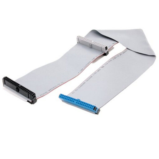 From

| Pin | Signal |
|---|---|
| 1 | Reset |
| 2 | Ground |
| 3 | Data 7 |
| 4 | Data 8 |
| 5 | Data 6 |
| 6 | Data 9 |
| 7 | Data 5 |
| 8 | Data 10 |
| 9 | Data 4 |
| 10 | Data 11 |
| 11 | Data 3 |
| 12 | Data 12 |
| 13 | Data 2 |
| 14 | Data 13 |
| 15 | Data 1 |
| 16 | Data 14 |
| 17 | Data 0 |
| 18 | Data 15 |
| 19 | Ground |
| 20 | Unconnected |
| 21 | DDRQ |
| 22 | Ground |
| 23 | I/O write |
| 24 | Ground |
| 25 | I/O read |
| 26 | Ground |
| 27 | IOCHRDY |
| 28 | Cable select (grounded) |
| 29 | DDACK |
| 30 | Ground |
| 31 | IRQ |
| 32 | Unconnected |
| 33 | Addr 1 |
| 34 | GPIO_DMA66_Detect |
| 35 | Addr 0 |
| 36 | Addr 2 |
| 37 | Chip select 1P |
| 38 | Chip select 3P |
| 39 | Activity |
| 40 | Ground |
Weirder shapes
In more complex case, the ground can have a non regular shape, either to achieve a particular effect, or just a convenience.
A first example is this schme I used a few years before to achieve the impedances I wanted while keeping the trace widths I wanted. The ground plane with the ground and the metalic part on which it is attached behave as a single ground conductor.

A second example are hybrid modules. Here, inputs and outputs have coaxial shapes, ground is all around all sections of the circuits, and a ground plane is provided everywhere.
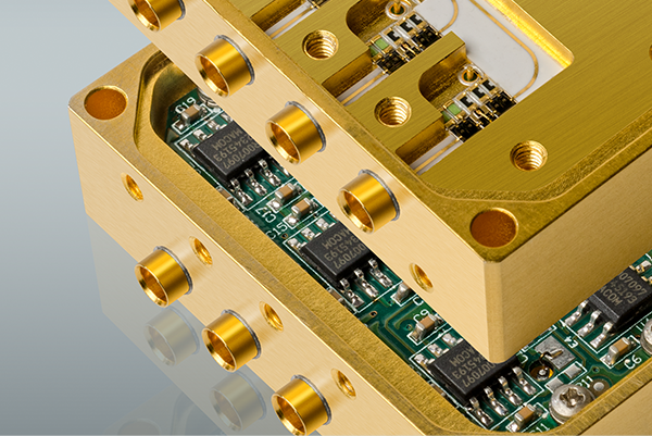 Copyright SemiGen, https://www.semigen.net/about/
A derivation of rules
Connections inside PCB
Horizontal PCB connections
It can be safely assumed that the optimal grounding scheme for systems where frequency high enough dominate (> 1 MHz), that is most of the systems, would be to have coaxial cables between each functional block. Even if this scheme is totally unpacticable at the board level, it can be approximated by following a few rules.
It can be shown mathematically that a coxial line is equivalent to a microstrip line with an infinite ground plane and all other signal being on the other side of the ground plane. This might seem inconvenient at a first glance, but note that it is a common practice to put on different sides of ground planes signals which would be very likely to perturbate each other.
A good approximation is to have microstrip lines with ground plane extending at least 5 times the substrate thicknes (or 3 times if relaxed) around the line, and to have nearby line no closer than the same amount. Once again, common PCB design rules.
Vertical PCB connections
The careful reader would have noticed that the previous rules solved the case of horizontal propagation in the PCB, but not the case of layer to layer propagation. Hence the base “coax rules” provides again answers: the ideal coxial line between the layers turns to be simple stitching vias, for simple case, or a full coaxial circle of vias for very high (> 10 GHz) frequencies.
PCB to outside connections
Coaxial connectors
A straightforward application of the coaxial ideal is the use of RF coaxial connectors or BNC connectors typically used for the low frequency signals (also by tradition, BNC connectors works work without any problem beyond 1 GHz), either directly screw-mounted to the chassis or connected through an intermediate coaxial cable to it.
Low frequency signals (e.g. banana plugs)
Lower frequency wires, not always using coaxial connectors, when then are referrenced to a ground, should always be accompagnied by a ground wire connected on both sides. Not doing this creates typically large loops, either large current loops producing radiation, or large loops receiving radiation.
The case of isolated wires, typically the red and black connector of an isolated power supply, won’t be covered here, but a viable strategy could be to treat them as two coupled signals with a common ground conductor grounded on both sides.
Ground connections between PCB and case
While some particular configurations might benefit from a single point grounding, more often this configuration is unpracticable. According to the “everything should be coax” rule if ground is connected in a single point, every signal should also follow this connection, like in the following picture from Ott:
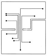
Let aside the inside of PCBs where this could be convenient, for the PCB to outside case, the signals have more often than not connectors big enough so that the bunch of connectors cannot be considered as a single point, at least at higher frequencies, like in the following picture from Spectran.
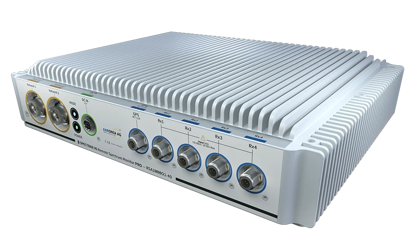
Also, for convenience or due to external constraints, the various connectors can even be on different sides.
Each signal connection should have its ground, so multiple point grounding occur naturally.
Conclusion
Most good practices of grounding and shielding signals can be derived starting from an approximation of using coaxial cables for each signal. Each signal must have a ground. Ground planes are the go-to way to provide this on PCBs. But variants exists and are sometimes very convenient. Mesh grounding occurs naturally.