Design of a coaxial power combiner with low-impedance inputs and increased isolation.
11 Apr 2022Hadrien Theveneau, Christophe Gaquière, Romain Lenglet, Matthieu Werquin, Jean-Christophe Joly, and Stéphane Tortel
This post is a mix between an unpublished long article, an article published in IEEE MWCL1, and further additions. Original articles by the authors in front of this post, revisions by the first author.
Introduction
More and more applications need to generate very high power pulsed microwave signals, in the order of tens of kilowatts: radars, EM warfare, and so on. These powers are traditionally generated with hyperfrequency tubes: magnetrons, klystrons, TWT, and so on. However, these techniques can have several major drawbacks: poor reliability, short lifespan, fragility, complex waveforms generation difficult and difficult power supplies.
Gallium nitride (GaN) transistors can provide a solution to these problems. However, the output power of a single transistor unit is insufficient for such applications. Efficient power combining schemes must be used to provide needed output power.
However, current solutions have limitations. Spatium® power combiners2,3 confine the amplifiers inside the structure, which makes thermal cooling difficult. Combiners using probes in linear waveguides4, coaxial waveguides5,6, or radial waveguides7 have low losses but their bandwidth is lower than 50 % and are not practical for lower frequencies like 1 GHz. These solutions also lack isolation between the inputs, which can lead to instability and failure propagation problems. Waveguide combiners8 have low losses and isolate their inputs, but they also have bandwidth limitations, and are bulky for lower frequencies. All of the previously mentioned solutions have high-impedance inputs (50 Ω), difficult to match on the low impedances (≈ 2.5 Ω) of GaN power transistors on large bandwidths
In this article, an innovative spatial power combiner with high bandwidth, isolation between its inputs and low input impedance is designed, manufactured, and measured. Section I presents a theoretical analysis of the lack of isolation of traditional power combiners, section II presents the general architecture of this new combiner, section III presents equivalents schematics in even and odd modes, section IV shows the structure of impedance prematching used to have low-impedances inputs, section V gives the complete procedure to calculate the shape of the impedance transition, and section VI discusses measurement and simulation results.
I. Even and odd modes analysis of power combiners
We will show in this section that the lack of isolation of power combiners without an isolation mechanism is linked to the reflection of the odd modes.
Fig. 1. shows the even and odd mode excitations of a power combiner without isolation mechanism. In the even mode, the power of the inputs goes to the output. If the impedance matching is correct, no output is reflected to the inputs and they don’t see each other. However, in symmetrical odd modes, due to symmetry, the output is connected to a virtual ground. The input waves are totally reflected. This reflection is the cause of the lack of isolation between the inputs. To provide isolation between the inputs, we need to find a way to absorb this reflection. Similar analysis is done in [9] and [10] for combiners using several discrete resistors.
Mathematically, for a combiner with rotational symmetry, the input modes matrix is given by:
where N is the number of inputs. The first column is the normal combining mode, the even mode, while the other columns are the odd modes.
For example, for 2 and 4 inputs, M is given by:
The inverse of M is given by:
By splitting the input excitation in even and odd modes, the isolation can be calculated as following :
where
II. Overview of the combiner
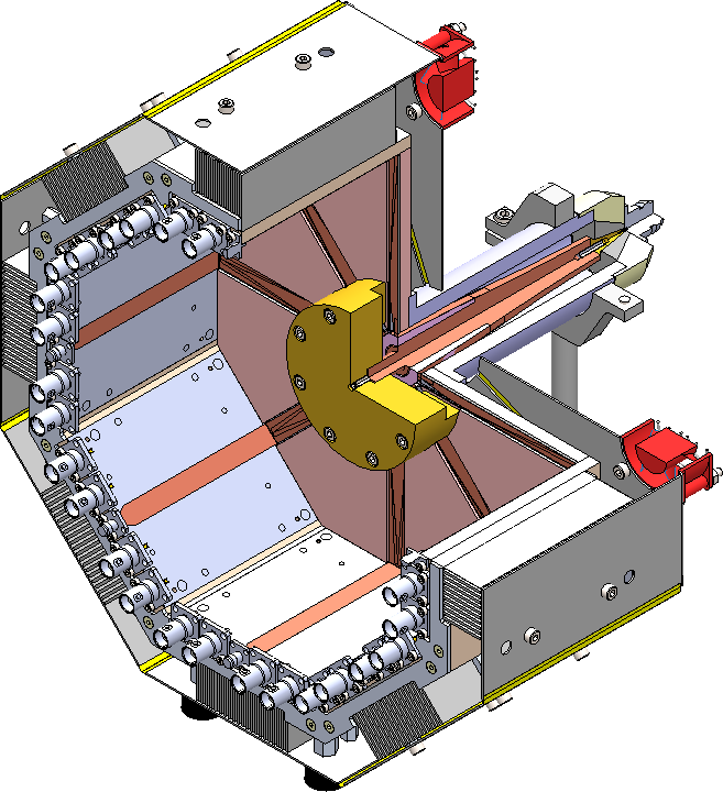
The mechanical layout of the power combiner is presented in Fig. 2. and Fig. 3. Standard 50 Ω connectors are present for measurement purposes, but this combiner is designed for 2.5 Ω inputs. These connectors will be eventually replaced by amplifier modules with low impedance outputs.
Impedance prematching networks raise the input impedance from 2.5 Ω to 50 Ω. This provides a sufficiently high impedance at the start of the combining section to avoid short distances between the inner part of this section and the outer part. Without the prematching, this distance would be on the order of 120 µm, which is very difficult to manufacture. With the prematching, this distance is between 0.8 and 1.9 mm, which is much easier to manufacture.
The actual combining11 begins after the prematching. The first part of the combiner is a coaxial structure containing several copper lines around an absorber material. This provides isolation between the inputs by adding some loss mechanism for the odd modes. Without this, the odd modes would be reflected back to the inputs, and this would cause the poor isolation found in lossless combiners. This absorber is similar to the resistor in Wilkinson combiners12,13,14,9, but its distributed operation provides an higher bandwidth.
Inside the absorber, there is a metal core connected to the body of the combiner. This provides a return path for the heat generated into the combiner. This metal core increases insersion losses of the combiner, particularly in the low frequency range, but this effect is low. Without this return path, the combiner would not be able to sustain high powers. Additionally, this structure allows mechanical sustaining.
The shape of the combining section is precisely calculated to ensure impedance matching between the inputs and the output. This calculation will be described in section V
At the exit of the combining section, there is one transition between air and PEHD, and one transition in diameter. No impedance matching is performed in these transitions: they have no electric function and are purely mechanical. The PEHD is here to ensure the positioning of the core inside the coaxial structure. The output coaxial connector alone would be insufficient to provide enough mechanical strength. Both transitions were optimized in separate EM simulations.
A CAD of the combiner with the power amplifier modules is shown in Fig. 4. A dummy circuit is shown in the figure to make mechanical CAD easier. Special care was taken with the cooling of the modules because the average lifespan of a GaN transistor is divided by 2 for each 6~°C increase in temperature. Unlike Spatium® power combiners2,3, where the power amplifiers MMICs are trapped inside the structure, the transistors are mounted on the outer part and thus can be more easily cooled. The overall structure is contained in a 333×322×286×mm3 volume.
III. Equivalent schematics in even and odd modes
The simplest method to analyse this power combiner is to use two separate schematics for the even mode and the odd modes, as shown in Fig.~\ref{fig-sch-even-odd-combiner}.
The prematching section behaves in exactly the same way in the even and the odd modes. Its equivalent schematic is a transmission line of continuously variable impedance. Its structure will be detailed in Fig. 7.
|
|
|
|
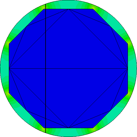
In the even mode, as shown in Fig. 5a, the strips have the same potential and almost no field goes into the absorber. The lines have low losses and the even mode is transmitted from point A to point B. The rest of the combiner, made with a full metal core, completes the impedance transformation, which was started in the prematch section. The heat spreader behaves approximately like a shunt inductor. This mode is the normal combing mode.
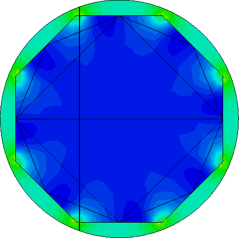
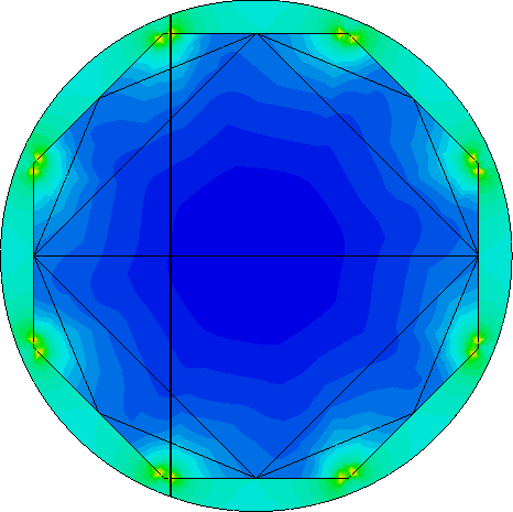
In contrast, in the odd modes, as shown in Fig. 5b and Fig. 5c, the strips do not have the same potential and lots of electric field goes into the absorber. The lines have high losses and the odd modes are highly attenuated from point A to point B.
In the odd modes, due to symmetry, point B behaves like a virtual ground. The heat spreader can be removed from the odd modes’ equivalent schematic because it is connected to the virtual ground. Without the absorber, the odd mode would be reflected towards the inputs. This reflection would cause a lack of isolation. With the absorber, the reflection of the odd modes is strongly attenuated, which increases isolation between the inputs. This absorber has the same function as the resistor in Wilkinson combiners12,13,14,9, but its distributed operation provides higher bandwidths.
IV. Impedance prematch
This combiner has an impedance preadaptation from 2.5 Ω to 50 Ω to make the manufacturing easier. This adaptation cannot be performed with a microstrip line on substrate with constant thickness. The 2.5 Ω low impedance side has a limited width because, otherwise, higher order modes would propagate. Using high-k substrates is not a solution because they would reduce the maximal width relative to the propagation of higher order modes. This forces the use of a thin substrate. However, a thin substrate forces the use of a narrow strip on the 50 Ω high impedance side, limiting the power handling and increasing the losses.
We need some way to change the thickness of the substrate. Using multiple substrates can be difficult for the manufacturing. A continuous variation of the thickness of the substrate would be difficult to manufacture. This is why we use a defective ground plane16,17,18,19. Fig. 7. shows the structure of the impedance preadaptation. The ground plane is progressively opened to increase the “effective substrate height”. The ground plane is opened before the strip width is reduced to have minimal losses. Impedance in function of dimensions is computed using the mode solver of CST Microwave Studio®.
V. Calculation of impedance transition
After the manufacturing of this combiner, the author learned that instead of a Klopfenstein transform followed by a postprocessing to remove the discontinuities, an Hecken transform should have been used instead. Hence, the first section presents what was done and the seconde section presents what should have been done instead.
V.I. Current calculation with Klopfenstein
A Klopfenstein impedance transition20,21,22,23,24,25 is used for this power combiner. The impedance preadaptation and the combining sections together make a single Klopfenstein impedance transition. Putting two Klopfenstein transitions in series would have been easier to calculate, but this would have increased the length and the losses of the overall structure.
The preadaptation section is the 2.5 Ω to 50 Ω part of a Klopfenstein transition going from 2.5 Ω to 8×50=400 Ω. The combining section is the 50/8=6.25 Ω to 50 Ω part of a 2.5/8=0.31 Ω to 50 Ω Klopfenstein transition. Both transitions are identical besides a multiplication of the impedance by 8, the number of the lines. This is because, in the prematching section, the impedance is the impedance of a single line, while in the combining section the impedance is the common-mode impedance of all the lines in parallel. Klopfenstein transitions are much discussed in literature20,21,22,23,24,25, but some points deserve special attention. The following procedure is used for the calculation:
1) Impedances Z(y) are calculated in function of the normalized position y in range [-1;1] using standard formulas for Klopfenstein transitions20,20,21,22,23,24,25.
2) An affine transformation was performed on
3) The electrical length of the transition,
4) The calculated impedances
5) A table of the
6) Profile transverse dimensions are calculated from
7) Position z is calculated from
by numerical integration. Fig. 8. shows the variation of the different parameters of the transition.
8) The number of points is reduced from 2001 to fewer than 20 points using an iterative end-point fit algorithm. This simple step is very important. Without this step, the mesher would not be able to mesh the structure for numerical simulation. This also helps manufacturing a lot.
V.I. Correct calculation with Hecken method
Instread of a modified Klopfenstein transition, the calculation method can be updates to use an Hecken transition. For this, at step 1,
VI. Simulation and measurement results
To validate the performance of the design before manufacturing, we perform a global electromagnetic simulation. The model includes the initial microstrip lines, the impedance prematching, the combiner itself and the final diameter reduction. SMA input connectors are not considered in this simulation because they are used for measurements only and should be removed for use with 2.5 Ω power amplifier modules. Their effect is removed from the measurement results. The output connector is also not considered because its effect is low compared to the other losses.
Separate CAD models are used for the mechanical manufacturing and the electromagnetic simulation. The use of two separate models is mandatory because the electromagnetic model and mechanical model have different requirements. For example, the screws must be included in the mechanical model, but they are ignored in the electromagnetic model.
The simulation is performed with CST Microwave Studio®. We use the frequency domain solver with tetrahedral meshing, automatic meshing and meshing adaptation. This simulation and meshing method are used because they allow both small and large features to be considered in the same simulation. The smallest features are present in the input microstrip lines, made on 127 µm substrate, and largest are present at the end of the combining, whose diameter is 30 mm.
Measurements of this power combiner are very difficult because the inputs are wide microtrip lines with low-impedances. Neither commercial connectors nor measurement instruments can directly connect to such inputs. For the measurements, we manufactured and measured a test version with standard 50 Ω SMA female connectors as inputs.
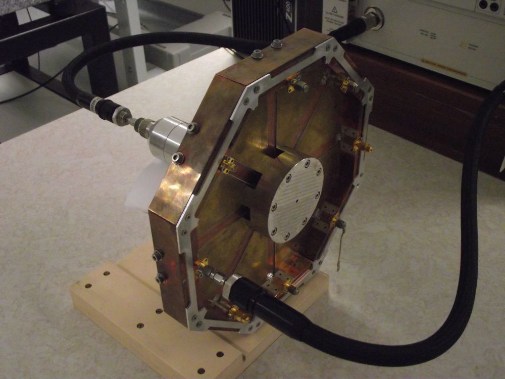
This test version is measured with a standard 50 Ω vector network analyser. The measurement setup is shown in Fig. 9. It is made two ports at a time with the remaining ports loaded with matched 50 Ω loads. The N to SMA transition at the 50 Ω output is simply ignored. A Python script using scikit-rf library is used to combine the multiple Touchstone 2-port files into a single 9-port file. The &&S_{i,j}&& coefficients measured several times, e.g. &&S_{1,1}&&, are averaged between all measurements. De-embedding and impedance renormalization are performed with Keysight Advanced Design System.
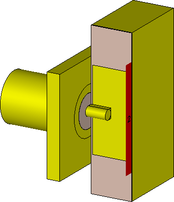
The transitions from the 50 Ω SMA coaxial connectors to the 2.5 Ω wide microstrip lines, present in the test version of the combiner, need to be desembedded. This desembedding is done using the simulated EM model of the transition shown in Fig. 10.
Measurement results after desembedding and impedance renormalization are shown in Fig. 11, Fig. 11, Fig. 12, and Fig. 13, along with the simulation results. Combining losses (Fig. 11) are lower than 1.8 dB on a 1 – 6 GHz band, except a few peaks. These peaks are due to mechanical tolerances in the start of the combining section, where minimal distance between parts is only 0.8 mm, and can be removed by a redesign of this combiner, by increasing this small dimension. This figure is good because it includes the impedance preadaptation from 2.5 Ω. RMS phase error of the inputs (Fig. 12) is lower than 15° on the full band. These two parameters, insertion loss and RMS phase error, are very promising for power combining.
The worst case isolation between inputs is at least 10 dB for inputs close to each other (45° pair) and at least 15 dB for other pairs. This isolation enables instability problems to be avoided, and enables the propagation of a failure from a device to another one to be avoided. If a power amplifier module fails, the system can be operated at a reduced power with the other power modules, compared to TWTA-based solutions.
Power handling of this combiner is difficult to measure, because the spatial distribution of thermal losses is not the same in splitting and combining modes, and the inputs cannot be directly connected to standard coaxial 50 Ω amplifiers. The power handling is estimated by an electro-thermal simulation. Fig. 15a. shows the temperature of the device for a combined input power of 500 W CW at 1 GHz. This frequency is the worst case for thermal effects. Output power is 330 W CW and maximal temperature is 225 °C in the absorber. The current version uses an MF124 absorber, able to withstand a maximum temperature of 180 °C, which gives a maximal output power of 260 W at 1 GHz. This power can be easily increased to 380 W using a MF500-124 absorber, withstanding 260~ °C.
Fig. 15b. shows the temperature of the device when the top input is turned off. Maximal temperature is 259 °C in the absorber.
Table 1. shows comparison with related power combiners. It is the only one which has low impedance inputs. Insertion losses are high, but such high losses are due to the combination of the high impedance transformation ratio and the low lower frequency.
| BW | N | Zin | IL | Isolations | Refs |
| [GHz] | [dB] | [dB] | |||
| 1 - 6 | 8 | 2.5 | 1.7 | 11.5 20.1 18.9 17.2 | This work |
| 2 - 8 | 8 | 50 | 0.4 | 9.5 17.0 16.3 12.7 | 26 |
| 2 - 17 | 8 | 50 | 1 | 9.5 17.0 16.3 12.7 | 26 |
| 7.6 - 10.4 | 12 | 50 | 1 | - | 27,28 |
| 5 - 20 | 64 | 50 | 1.5 | - | 29 |
| 6 - 18 | 20 | 50 | 0.97 | - | 25 |
| 2 - 16 | 32 | 50 | 1.2 | - | 30 |
| 0.52 - 1.86 | 8 | 50 | 0.2 | - | 31 |
| 12.1 - 15.7 | 8 | 50 | 0.17 | 7.0 12.0 11.0 7.0 | 32 |
| 8 - 18 | 8 | 50 | 0.5 | 9.0 7.2 10.2 11.0 | 33,7 |
| 28 - 36 | 20 | 377 | 1.0 | 12.0 15.0 17.0 18.0 | 8 |
| 11.5 - 16 | 8 | 50 | 0.5 | 9.0 14.6 22.6 16.3 14.6 | 8 |
Conclusion
A 1 – 6 GHz spatial power combiner with 2.5 Ω low-impedance inputs and increased isolation had been designed, manufactured and measured. Total losses, including impedance prematch, are lower than 1.8 dB, except on a few peaks. These peaks are due to mechanical tolerances and can be removed by increasing some critical dimensions.
This new power combiner is very promising for high power (kW) combining in a wide frequency range. Thanks to the low insertion losses, the impedance pre-matching, the ability to evacuate calories of the active devices, and the isolation between the inputs.
This design is the subject of the European patent “Spatial power combiner” number EP3171451A1.
Acknowledgments
The authors would like to thank Sylvie Lepilliet of the IEMN for her precious help during the measurements, Pierre Bruguière of the CEA for reviewing, CST for its cooperation, Steve Huettner and Terry Cisco of Microwaves101 for good advice, and Steve Arscott of the IEMN for help with English language.
-
Hadrien Theveneau, Christophe Gaquière, Romain Lenglet, Matthieu Werquin, Jean-Christophe Joly and Stéphane Tortel, Spatial Power Combiner With Low-Impedance Inputs and Increased Isolation, in IEEE Microwave and Wireless Components Letters, vol. 27, no. 11, pp. 956-958, , DOI: 10.1109/LMWC.2017.2750100. Available: https://www.researchgate.net/publication/320070246_Spatial_Power_Combiner_With_Low-Impedance_Inputs_and_Increased_Isolation ↩
-
P. Jia, L.-Y. Chen, A. Alexanian, and R. York, “6 to 17 ghz broadband high power amplifier using spatial power combining technique,” in Microwave Symposium Digest, 2003 IEEE MTT-S International, vol. 3, , pp. 1871–1874 vol.3. DOI: 10.1109/MWSYM.2003.1210521. ↩ ↩2
-
P. Jia, L.-Y. Chen, A. Alexanian, and R. York, “Broad-band high-power amplifier using spatial power-combining technique,” IEEE Transactions on Microwave Theory and Techniques, vol. 51, no. 12, pp. 2469–2475, . DOI: 10.1109/TMTT.2003.819766 ↩ ↩2
-
L. A. Li, B. J. Hilliard, J. R. Shafer, J. Daggett, E. J. Dickman, and J. P. Becker, “A planar compatible traveling-wave waveguide-based power divider/combiner,” IEEE Transactions on Microwave Theory and Techniques, vol. 56, no. 8, pp. 1889–1898, . DOI: 10.1109/TMTT.2008.926555. ↩
-
D. I. L. de Villiers, P. W. van der Walt, and P. Meyer, “Design of conical transmission line power combiners using tapered line matching sections,” IEEE Transactions on Microwave Theory and Techniques, vol. 56, no. 6, pp. 1478–1484, . DOI: 10.1109/TMTT.2008.923879. ↩
-
K. Song and Q. Xue, “Planar probe coaxial-waveguide power combiner/divider,” IEEE Transactions on Microwave Theory and Techniques, vol. 57, no. 11, pp. 2761–2767, . DOI: 10.1109/TMTT.2009.2032483. ↩
-
K. Song, Y. Fan, and Z. He, “Broadband radial waveguide spatial combiner,” Microwave and Wireless Components Letters, IEEE, vol. 18, no. 2, pp. 73–75, . DOI: 10.1109/LMWC.2007.911984. ↩ ↩2
-
Q. X. Chu, D. Y. Mo, and Q. S. Wu, “An isolated radial power divider via circular waveguide te01-mode transducer,” IEEE Transactions on Microwave Theory and Techniques, vol. 63, no. 12, pp. 3988–3996, . DOI: 10.1109/TMTT.2015.2495204. ↩ ↩2 ↩3
-
W. Yau, J. Schellenberg, and Y. C. Shih, “A new n-way broadband planar power combiner/divider,”in 1986 IEEE MTT-S International Microwave Symposium Digest, , pp. 147–149. 10.1109/MWSYM.1986.1132133. ↩ ↩2 ↩3
-
Nobuo Nagai, Eiji Maekawa et Koujiro Ono. “New n-Way Hybrid Power Dividers”. In: IEEE Transactions on Microwave Theory and Techniques, 25.12 (), p. 1008–1012. ISSN : 0018-9480. DOI : 10.1109/TMTT.1977.1129265. ↩
-
In this article, we use the term “combiner” loosely for both the complete system, including the impedance prematching, and the mere combining part, without prematching. ↩
-
The Unknown Editor, “Wilkinson power splitters”, , P-N Designs. Available: https://www.microwaves101.com/encyclopedias/wilkinson-power-splitters. ↩ ↩2
-
S. B. Cohn, “A class of broadband three-port tem-mode hybrids,” IEEE Transactions on Microwave Theory and Techniques, vol. 16, no. 2, pp. 110–116, . DOI: 10.1109/TMTT.1968.1126617. ↩ ↩2
-
E. Wilkinson, “An n-way hybrid power divider,” IRE Transactions on Microwave Theory and Techniques, vol. 8, no. 1, pp. 116–118, Jan. 1960. DOI: 10.1109/TMTT.1960.1124668. ↩ ↩2
-
Hadrien Theveneau, “Amplificateurs de puissance à transistors GaN,” available: https://www.researchgate.net/publication/314102156_Amplificateurs_de_puissance_a_transistors_GaN. ↩
-
A. Arbabi, A. Boutejdar, M. Mahmoudi, and A. Omar, “Increase of characteristic impedance of microstrip line using a simple slot in metallic ground plane, in First International Conference on Communications and Electronics, 2006. ICCE ’06. , pp. 478–481. ↩
-
A. Boutejdar, J. Machac, L. Haiwen, and A. Omar, “Miniaturized microstrip lowpass filter with wide stopband using suspended layers and defected ground structure (dgs),” in 14th Conference on Microwave Techniques, 2008. COMITE 2008. , pp. 1–4. ↩
-
Schlieter and R. Henderson, “Designing high impedance etched ground gcpw,” in Wireless and Microwave Technology Conference, 2009. WAMICON ’09. IEEE 10th Annual, , pp. 1–4. ↩
-
J. Lim, D. Ahn, S.-M. Han, Y. Jeong, and H. Liu, “A defected ground structure without ground contact problem and application to branch line couplers,” International journal of antennas and propagation, vol. 2013, no. 232317, p. 5 pages, . DOI: 10.1155/2013/232317. Available: https://www.hindawi.com/journals/ijap/2013/232317/. ↩
-
D. Pozar, Microwave engineering. Hoboken, NJ: Wiley, . ↩ ↩2 ↩3 ↩4 ↩5 ↩6
-
R. Klopfenstein, “A transmission line taper of improved design,” Proceedings of the IRE, vol. 44, no. 1, pp. 31–35, Jan. 1956. DOI: 10.1109/JRPROC.1956.274847. ↩ ↩2 ↩3 ↩4 ↩5
-
R. Collin, “The optimum tapered transmission line matching section,” Proceedings of the IRE, vol. 44, no. 4, pp. 539–548, Apr. 1956. DOI: 10.1109/JRPROC.1956.274938. ↩ ↩2 ↩3 ↩4
-
D. Kajfez and J. Prewitt, “Correction to “a transmission line taper of improved design” (letters),” IEEE Transactions on Microwave Theory and Techniques, vol. 21, no. 5, pp. 364–364, . DOI: 10.1109/TMTT.1973.1128003. ↩ ↩2 ↩3 ↩4
-
The Unknown Editor, “Klopfenstein’s taper”, , P-N Designs. Available: http://www.microwaves101.com/encyclopedia/klopfenstein.cfm. ↩ ↩2 ↩3 ↩4
-
Y. Ning, W. Jiang, and W. Zhang, “The spatial power combining technique based on novel antipodal finline,” in IEEE International Wireless Symposium (IWS), 2013. , pp. 1–4. DOI: 10.1109/IEEE-IWS.2013.6616753. ↩ ↩2 ↩3 ↩4
-
M. Ghanadi, “A new compact broadband radial power combiner, Ph.D. dissertation, Elektrotechnik und Informatik der Technischen Universität Berlin, Berlin, 2012. ↩ ↩2
-
M. Cohn, B. Geller, and J. Schellenberg, “A 10 watt broadband fet combiner/amplifier, in IEEE MTT-S International Microwave Symposium Digest, 1979. , pp. 292–297. DOI: 10.1109/MWSYM.1979.1124047. ↩
-
J. Schellenberg and M. Cohn, “A wideband radial power combiner for fet amplifiers,” in IEEE International Solid-State Circuits Conference. Digest of Technical Papers. , vol. XXI, 02 1978, pp. 164–165. DOI: 10.1109/ISSCC.1978.1155840. ↩
-
A. Alexanian and R. York, “Broadband waveguide-based spatial combiners,” in IEEE MTT-S International Microwave Symposium Digest 1997. vol. 3, June 1997, pp. 1139–1142. DOI: 10.1109/MWSYM.1997.596528. ↩
-
P. Jia, L.-Y. Chen, A. Alexanian, and R. York, “Multioctave spatial power combining in oversized coaxial waveguide,” IEEE Transactions on Microwave Theory and Techniques, vol. 50, no. 5, pp. 1355–1360, . DOI: 10.1109/22.999150. ↩
-
M. Amjadi and E. Jafari, “Design of a broadband eight-way coaxial waveguide power combiner, IEEE Transactions on Microwave Theory and Techniques, vol. 60, no. 1, pp. 39–45, . DOI: 10.1109/TMTT.2011.2171499. ↩
-
X. Shan and Z. Shen, “A suspended-substrate ku-band symmetric radial power combiner,” IEEE Microwave and Wireless Components Letters, vol. 21, no. 12, pp. 652–654, . DOI: 10.1109/LMWC.2011.2173325. ↩
-
K. Song, Y. Fan, and Y. Zhang, “Broad-band power divider based on radial waveguide,” Microwave and Optical Technology Letters, vol. 49, no. 3, pp. 595–597, . DOI: 10.1002/mop.22216. ↩
 RF cat corner