 RF cat corner
On stability of capacitive loaded op-amps.
29 May 2025Introduction
Operational amplifiers are often, and for good reason, the go-to building block of many analog functions. They are often used with capacitive loads, for two main reasons. One, when operational amplifiers are used to produce DC voltage supplies, in which cases the capacitive load is used to ensure DC voltage stays constant. Second, when operational amplifiers are used to drive some capacitive load, typically the gate of the transistor of an RF power amplifier, including the capacitors of the biasing network.
However, a common trap with such circuits is that operational amplifiers tend to be unstable when they are capacitively loaded, even for relatively low values.
Beware of the “high capacitive load drive capability” op-amps
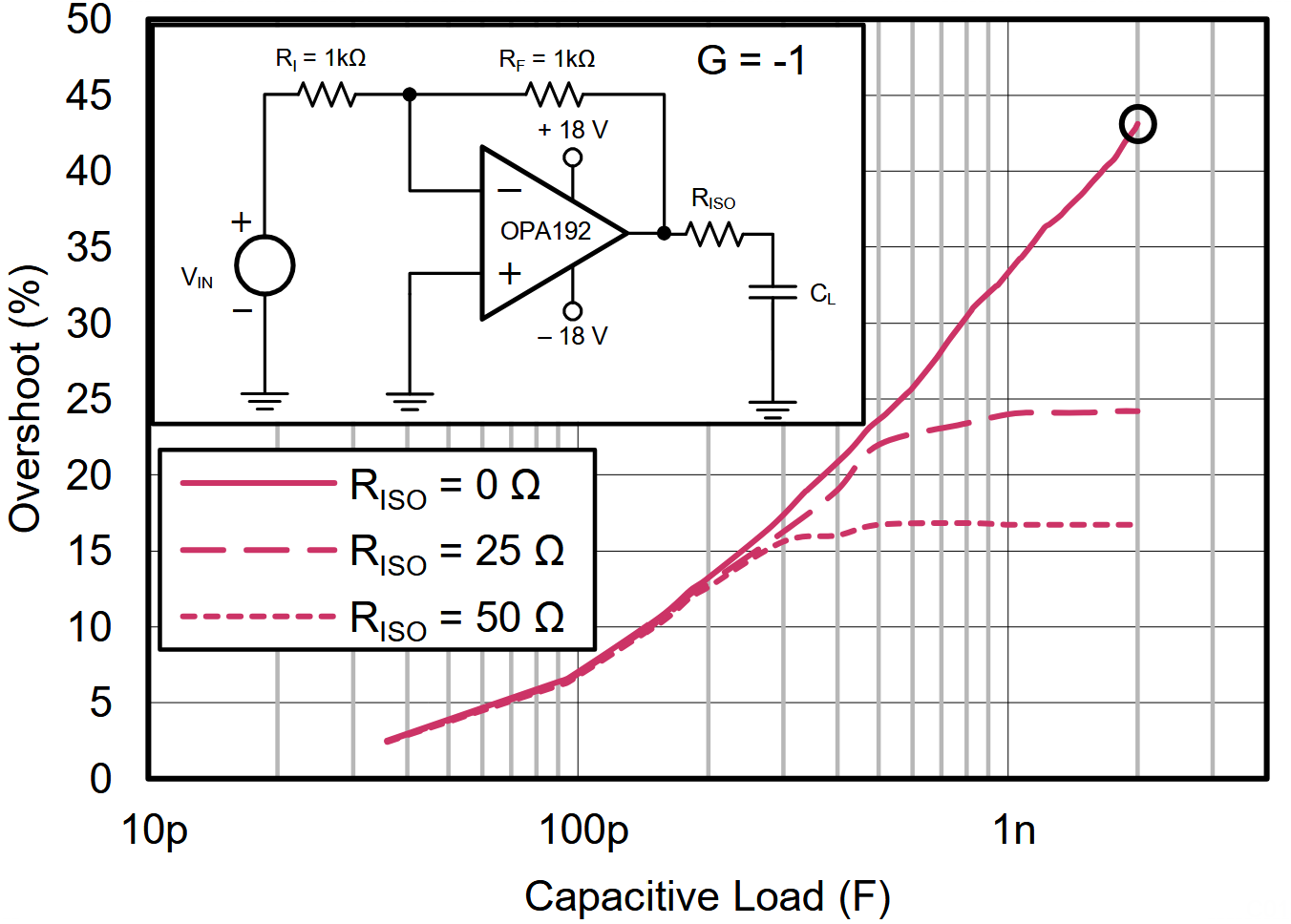
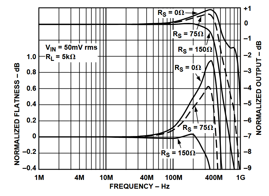
Some op-amps models like the OPA1921 advertise an “high capacitive load drive capability”, but the stated value is only 1 nF. Even if this is only a typical value, its conditions are rather fair: only 40% overshoot. The main problem is that it is only 1 nF.
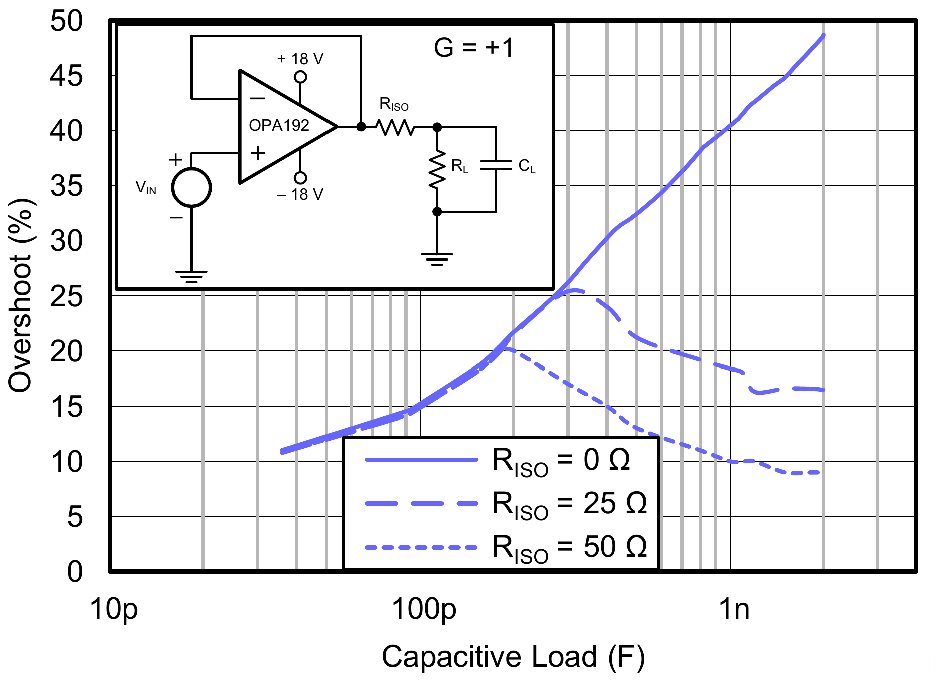
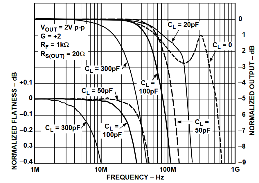
The same graphs suggest that a 25 Ω improves greatly the overshoot, with a maximum value of 25 %, and allows to use an arbitrarily high capacitive load.
And once the isolation resistor is added, it lacks only two components to make something perfect. Why not read the following and add them ?
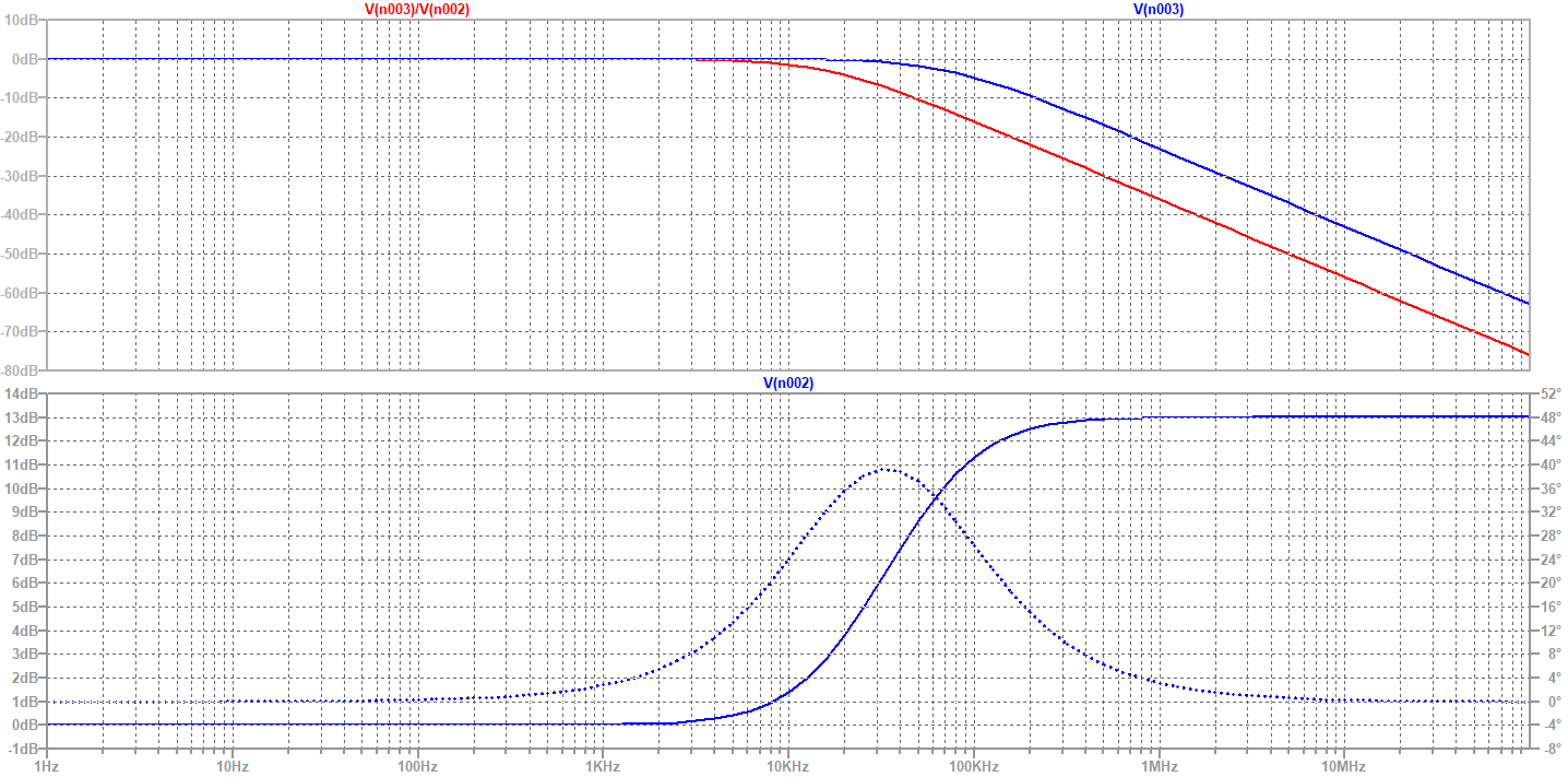
In the discussion, the OPA9942 was suggested. Indeed, it is advertised as having an “unlimited capacitive load drive capability” with a “phase margin of 50° when driving a load of 10 μF and 1 MΩ”. It is indeed the case. However, on some part of the phase margin plots, the phase margin is as low as 20°, and, again, is works much better with an isolation resistor. It should be noted, however, that the OP994 with a 50 Ω isolation resistor has a 45 % worst case overshoot while the OPA192 has only a 20 % overshoot.
|
|
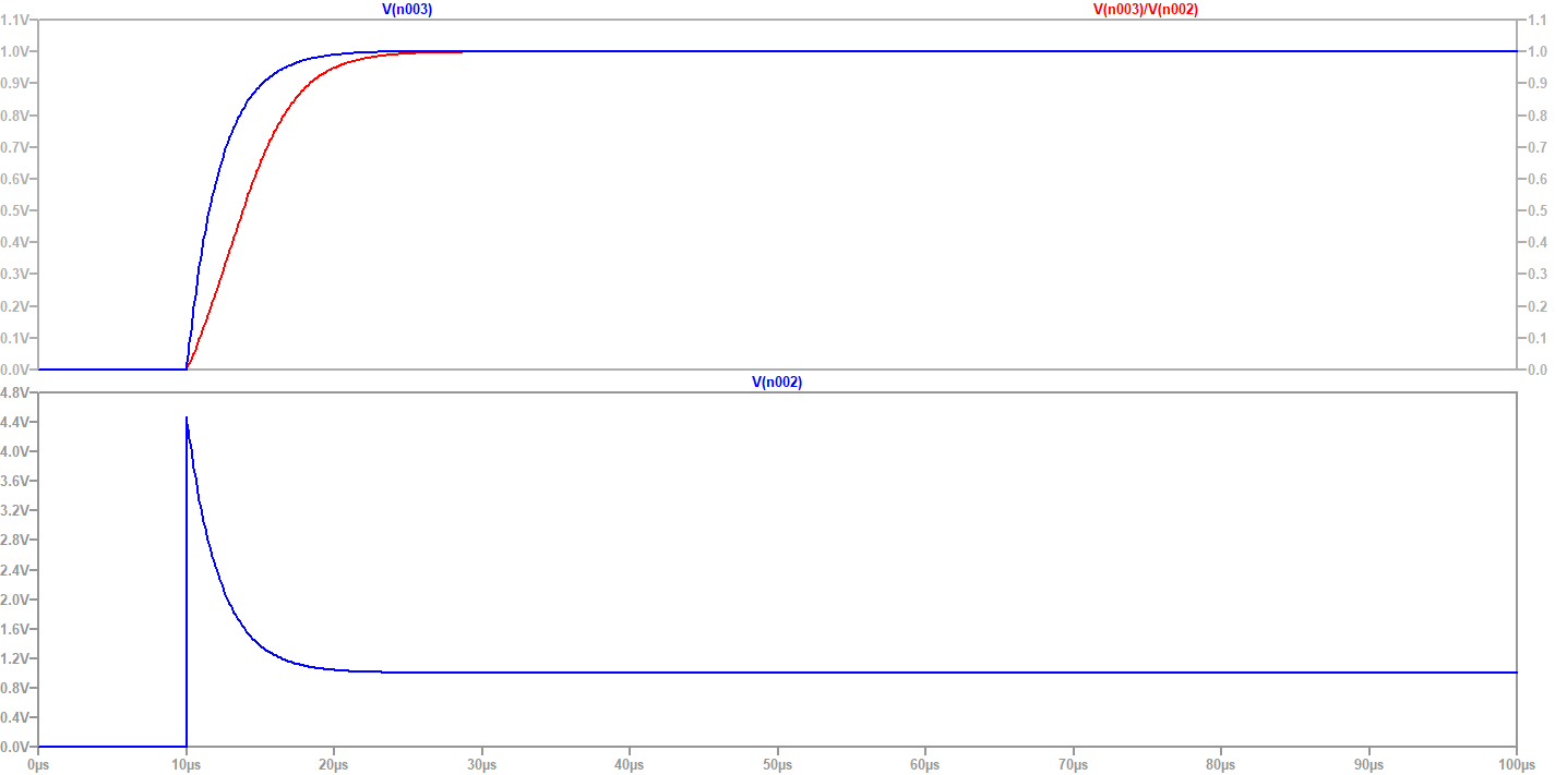
And once the isolation resistor is added, same comment than before.
The root cause
A feedback system must have less than 180° phase shift from its output to its - input at the unity gain frequency in order to the negative feedback to stay negative and to avoid it going positive and causing unstability. There are more complicated ways to tell this principle but the core concepts are here.
An ideal operational amplifier has already a -90° phase shift due to its integrator nature (the gain bandwidth product). Due to various unperfections, there is also a little more phae shifting. The open loop output impedance of the operational amplifier combined with the capacitive load easily makes almost -90° phase shift at unity gain if the GBW and the capacitor are high enough. All this combined, this can lead to high overshoots, an high closed-loop output impedance, or a caracterized oscillation.
Note what matter for stability is the open loop operational amplifier output impedance. The closed loop output impedance is much lower due to feedback, at least when the feedback operates properly.
Some details on the topic
The details of the topic won’t be explained here, because the most important is to be aware of the problem and of its solutions. Once the problem is known, details are easy to find on Google. Reference 3 is a great starter, even if I would suggest an other solution on the “RC filter directly at the input”, 4 gives more informations on threee useful solutions: RISO, RISO + DFB, RISO + DFB + RFx, 5 give more solutions and details, and 6 is a rather long presentation on the general subject of operational amplifier stability which beats the topic to death, 6 gives additional details and equations on the topic. This application note from Microchip7, although not complete on compensation networks, give useful equation, useful tips for ADC interfacing and give useful information on large signal effects.
The careful reader will probably notice a mistake in the “in-loop compensation circuit” of 5: Vin and GND are inverted, as well as the - and + inputs of the operational amplifiers. Despite this mistake, the remaining of the contents is highly valuable.
Important note on coaxial cables
A important case of “capacitive” loads are coaxial cables. Their distributed nature and associated characteristic impedance and propagation time makes it differ from purely capacitive loads in ways that should not ignored. Coaxial cables loaded by their characteristic impedance, most often 50 Ω, behave like like a pure resistance. Conversely, coaxial cables driven by with a source impedance equal to their characteristic impedance behave like a pure resistive source impedance.
When it is sure a coaxial cable would be loaded by its characteristic impedance, from a stability point of view, it is just a resistor. Nothing more is needed, provided the operational amplifier can feed the requested current.
When a coaxial cable is loaded by something looking like an open circuit, typically an high impedance digital input, it is best to source terminate it, by putting a resistor between the output of the operational amplifier, wired in the usual way, and the input of the coaxial cable. The coaxial cable will be merged with the source resistor, and all will behave like the source resistor loaded by the open circuit.
Such a scheme can also be used in cases where the load is most often an high impedance but not always, because the source resistor will ensure a minimum resistance seen by the operational amplifier and avoid stability problems.
In some cases, it can be useful to terminate the coaxial cable on both sides. This has the drawback to make the final voltage half the voltage at the output of the operational amplifier, but is a robust solution.
However, when the coaxial cable is loaded by some capacitor, they must together be handled like a capacitor. Nevertheless, due to the cable propagation time, some ringing can be expected if the rise and fall times are too small compared to it. This can be avoided by ensuring long enough rise and fall times or by adding some damping resistors.
Some comments of the common solutions
Input filtering
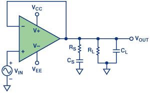
Not directly related to output driving load, this is nevertheless an interesting case to mention. Often it is derisable, particularly to reduce sensitivity to RFI and EMI, to filter the input. A capacitor straight at the op-amp inputs, like in figure below, is likely to make it unstable, for the reasons described above.
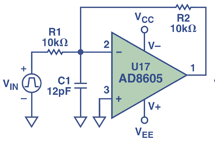
However, I would suggest an other solution than the one proposed by Analog Devices: splitting the input resistor and to put the filtering capacitor in the middle.
Output snubbing network
A perceived drawback of solutions using an isolation resistor is the voltage drop in the isolation resistor and the inability of using the full output voltage range of the operational amplifier, particularly for RRO (rail-to-rail-output) amplifiers.
Whether an isolation resistor is used or not, voltage margin between the desired voltage and the voltage rails of the operational amplifiers is useful so the retroaction loop can work properly.
In the case this solution must be used, like in the schematic below from Analog Devices, the principle can be explained in the following simple way. RS is low enough compared to CL to make the output load looks like resistive enough to ensure a good phase margin at the unity gain frequency, while CS is high enough compared to RS to make RS+CS close enough to only RS.
This solution stabilizes the circuit, but makes the load harder to drive, making this solution ok for DC or low frequency signals, but not so much for higher frequency cases.
A tricky point of this calculation is that the needed components values depends on the unity gain frequency, but it depends itself on the values of the snubber network which tend to reduce it.
Isolation resistor
An isolation resistor ensures the opamp sees at the unity gain a convenient load, either a low enough capacitance when the capacitive load is low enough compared to the isolation resistor, or the isolation resistor when the capacitive load is high enough. This ensures stability, but at a price: the opamp produced the wanted voltage with the feedback before the resistor, and the actual voltage at the load is RC filtered.
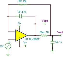
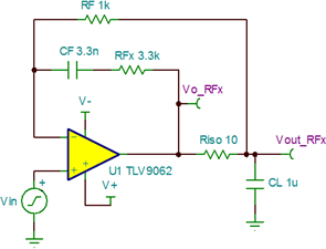
Isolation resistor + double feedback
This technique exists in two common variants shown in the 2 figures below from the excellent article4 from Texas Instruments.
|
|
The operating principle is the same in the two cases: provide an high frequency and a low frequency feedback paths. The high frequency path, right at the operational amplifier output, undelayed, provides stability, while the low frequency path, at the load, provided an exact low frequency response.
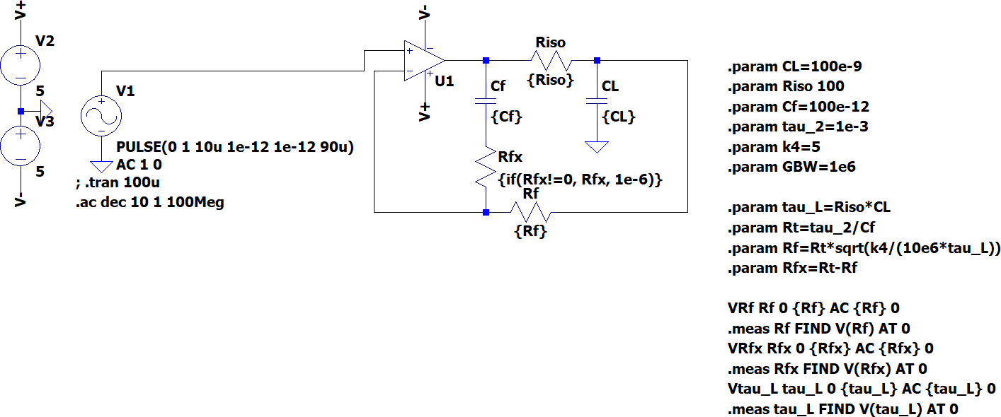
With some mathematics, it is possible to determine the optimum values which ensure both stability and performance. The detailed equations, rather long, are presented in this page: /posts/op-amp-capacitor-stability-equations.html.
Simulation results with the values calculated using the equations are shown below:
Some words on buffers
Unity gain buffer ICs can help to solve this problem, either as a standalone solution, when their offsets are tolerable, or as an addition to the opamp, kind of replacing the isolation resistors.
Since I had not yet the time to write on the topic, in waiting, please find a picture of this beautiful cat from Wikipedia:

Case studies
Sariel Hodisan
From this LinkedIn post8 from Sariel Hodisan:
Lately, I designed a simple biasing circuit for bipolar voltage rails (±13.5V) to bias a very precise low-noise analog circuit. To minimize offset in the analog section, it’s mandatory for the ±13.5V rails to be as closely matched as possible. The load is just a few mA, and it’s mostly a DC circuit. No fast current draws.
[...]
I did need decoupling for the biased circuit and figured 1nF would be enough. According to the OPA192 datasheet, there’s around 40 % overshoot when loaded with a [2nF, see below] cap.
[...]
The ±13.5V rails oscillated terribly.
Luckily, I had provisions to add an isolation resistor (30 ohm), and that solved the problem, though at the cost of a slight voltage drop.
I edited the message to make the total capacitive load more clear: 2 nF total, including 1 nF straight at the opamp output and 1 nF at the load.
Although some details are specific to his project, like his need of low noise, generating DC voltages to supply something is a very common need.
This circuit should not have oscillated so hard, according to the datasheet, which predicts less than 45 % overshoot for a 2 nF load.
He solved the problem using a simple isolation resistor, at the cost of a small voltage drop, and I suggested him to add a double feedback to eliminate the drop. Since it is a DC need, the simple double feedback is sufficient.
Microwaves101 gate pulser
In the excellent microwaves101 website9, a page is written on the subject of pulsed RF sources. Although it advises drain pulsing (this page was written long before before GaN was mainstream), it also gives some advice about gate pulsing (bold from myself):
For a good gate pulsing circuit, we recommend the Analog Device's AD8036 "clamping amp", shown below. It lets you set up on and off gate bias voltages independently; for example, if you are using a PHEMT power amp you can set VG(on) to -0.9 volts, and VG(off) to -1.5 volts. You still need charge storage on the drain bias lines, and stability caps on gate and drain biases, as near as possible to the amp. Like all op-amps, the AD8036 can be configured as an inverting or non-inverting amplifier. Yes, we need to add some resistive feedback to the figure!
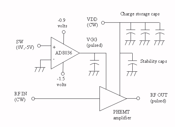
The feedback was forgotten in the figure, but not in the text.
However, a point which might need to be added is the stabilisation for capacitive loads. The AD8036 datasheet does not mention performance curves when capacitively loaded, but instead a recommended isolation resistor value:
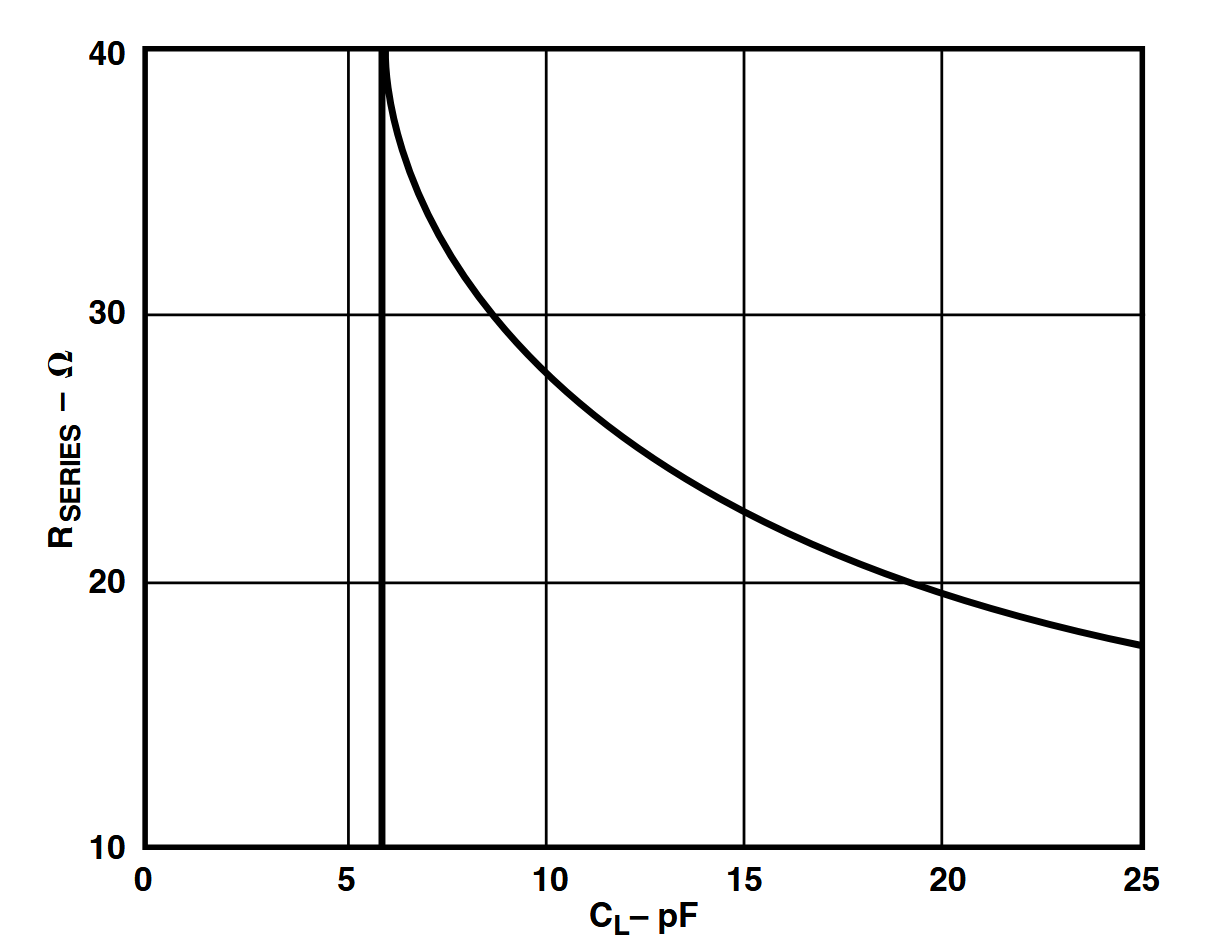
Given this curve and the typical gate bias network capacitance values, I would recommend a 20 Ω isolation resistor. The RC bandwidth is already 31.8 MHz. If not sufficient, a RISO + DFB + RFx can be used to both remove the RISO offset and to have speed up.
Microwaves101 gate pulser, alternative solution
That being said, we would propose here an alternative solution.
A problem with the AD803610 is that it is an input clamping amplifier, with clamping only available on its +VIN, making it “works only for noninverting or follower applications”. This needs a 0 to -5V input signal to have the requested VH and VL voltages. Not very convenient since most digital circuits operate on positive voltages.
Switching between two voltages levels would be conveniently done by a switch integrated circuit. Most common switches are slow, either because they are plain slow or because they include some “break before make” circuitry which take some transition times. The switches in the “buffered analog multiplexers” section of Analog Devices11 provide faster time, probably because the techniques to deal with switching transitions are easier to implement in unidirectional multiplexed buffer than in unidirectional buffer, like current steering:
The [ADV312912] multiplexer is organized as two input transconductance stages tied in parallel with a single output transimpedance stage followed by a unity-gain buffer. Internal voltage feedback sets the gain.
The following chips are interesting, with only single channel devices mentionned:
AD817013
AD818014
ADV321915
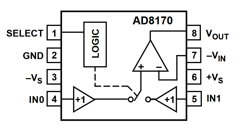
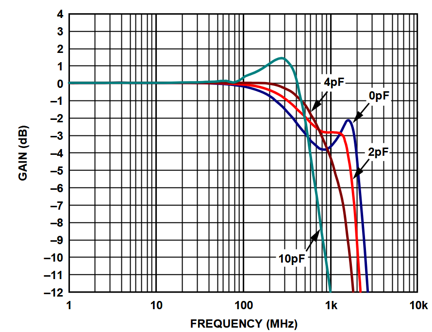
The AD8170 is a current feedback amplifier with a switchable input. These category of operational amplifiers are sensitive to the impedance seen at the feedback pin, to DFB schemes cannot be used directly with them. The datasheet recommands isolation resistor values and feedback resistance. Simple RC calculations shows that the performance is mainly determined by the RC constant of the isolation resistor and the capacitive load.
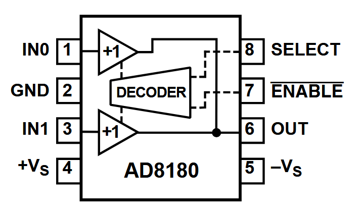
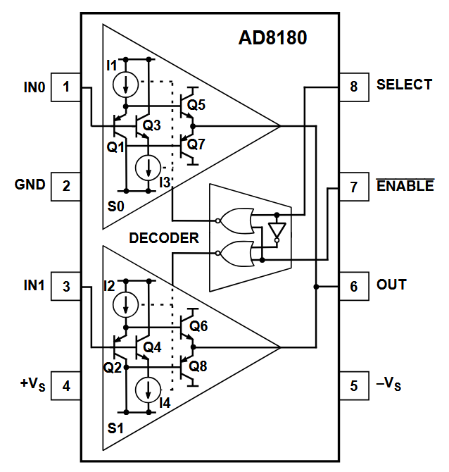
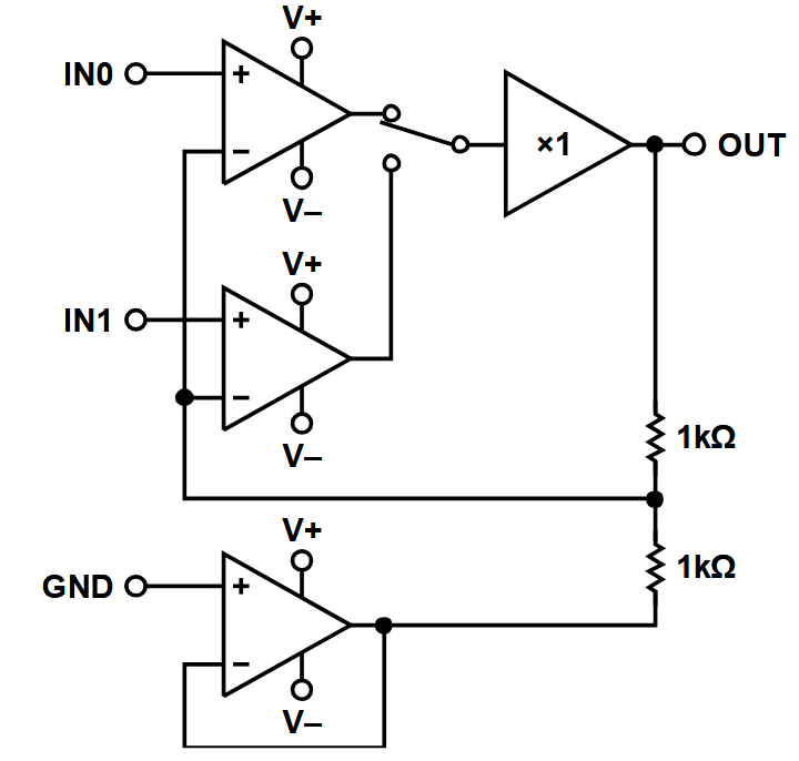
The AD8180 is an open loop buffer and can drive capacitive loads without isolation resistors. However, an input resistor is recommended. This is often the case for buffer amplifiers, and often forgotten. Performance is again determined by the open loop impedance of approximately 25 Ω.
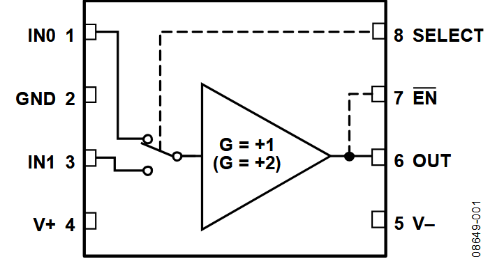
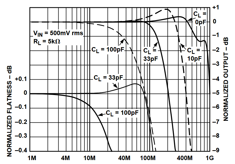
The ADV3219 is a feedback amplifier with an internal feedback. Performance curves are given for low capacitive loads without isolation resistor. For higher capacitive loads, the datasheets recommands an isolation resistor of “a few tens of ohms”, but does not give more performance details. Nevertheless it can be assumes that it will be dominated by the RC constant of the output.
|
|
AD8170 |
AD8180 |
AD8180 |
ADV3219 |
Conclusion
Capacitor unstability when capacitively loaded is a classical trap, catching even rather experienced designers, particularly RF designers who are not always proficient in low frequency analog design. Although it may seem hard, this problem is well known, well documented and has readily available efficient solutions.
Appendix
Previous version of the page included various cat pictures as placeholders for contents to be written. They are left here for posterity:
Courtesy of Microwaves101 (https://www.microwaves101.com/unknown-editor-121-cat-wrangler-april-2023):
From Wikipedia:

-
https://www.analog.com/en/resources/analog-dialogue/articles/techniques-to-avoid-instability-capacitive-loading.html ↩
-
https://www.analog.com/en/resources/analog-dialogue/articles/ask-the-applications-engineer-25.html ↩ ↩2
-
https://e2e.ti.com/cfs-file/_key/…/Solving_5F00_Op_2D00_Amp_5F00_Stability_5F00_Wells_5F00_6_2D00_5_2D00_12-_2800_2_2900.pdf ↩ ↩2
-
https://ww1.microchip.com/downloads/en/Appnotes/00884b.pdf ↩
-
https://www.microwaves101.com/encyclopedias/pulsed-rf-sources ↩
-
https://www.analog.com/media/en/technical-documentation/data-sheets/ad8036_8037.pdf ↩
-
https://www.analog.com/en/parametricsearch/11267#/sort=s3,asc ↩
-
https://www.analog.com/media/en/technical-documentation/data-sheets/ADV3219_3220.pdf ↩
-
https://www.analog.com/media/en/technical-documentation/data-sheets/ad8170_8174.pdf ↩
-
https://www.analog.com/media/en/technical-documentation/data-sheets/AD8180_8182.pdf ↩
-
https://www.analog.com/media/en/technical-documentation/data-sheets/ADV3219_3220.pdf ↩