Although it is still in draft stage, this document is released before finishing due to its interest. This page is a quick and dirty translation of a previous French document. Various editing issues are susceptible to be present.
A few words on the notion of transistor output impedance
In [PhD thesis section 16.1], we set aside the real behavior of power amplifiers to focus on the behavior of their loads, i.e., the inputs of the power combiner. Power amplifiers operating at high power are nonlinear, which causes particular effects on the behavior of their outputs. We will detail these effects in the following section.
Behavior of a simplified nonlinear power amplifier
Let us consider a simplified nonlinear amplifier. We will initially assume that it reacts instantaneously to its inputs, i.e., its response is frequency-independent. The model will be extended to incorporate frequency variations in the following section. Suppose its response can be described in the time domain by the equation below:
b_2(t) = \underbrace{G \cdot a_1(t)}_{\text{Gain in small signals}} - \underbrace{\gamma \cdot a_{1}^{3}(t)}_{\text{Gain compression}} + \underbrace{\Gamma \cdot a_2(t)}_{\text{Output reflection in small signals}} - \underbrace{\lambda \cdot a_{1}^{2}(t) \cdot a_2(t)}_{\text{Variation of reflection with input, self-biasing}}
This model is highly simplified but already contains the effects found in real amplifiers: small-signal gain, gain compression for large signals, output reflection, self-biasing, and variation of the output reflection coefficient as a function of input power.
For numerical examples, let us take the following values:
Figures \ref{fig-plt-non-lineaire-b2-a1} and \ref{fig-plt-non-lineaire-r2-a1} show respectively the instantaneous value of the output b_2(t) and the instantaneous reflection coefficient \frac{db_{2}(t)}{da_{2}(t)}, both as a function of the input a_1(t).
Output b_2(t) as a function of input a_1(t).Instantaneous reflection coefficient \frac{db_{2}(t)}{da_{2}(t)} of the output as a function of input a_1(t).
This nonlinear equation can be linearized [1,2] around an operating point, which we will call “LSOP” for “large signal operating point”. This operating point is:
We ignore the terms in e^{3 i \omega t} and e^{-3 i \omega t} which correspond to the third harmonic of the signal, and we are interested in the amplitude of the terms in e^{i \omega t} and e^{i \omega t}:
b_{2}(t) = \frac{ B_2 \cdot e^{i \omega t} + B_{2}^* \cdot e^{- i \omega t} }{2} + \text{terms in } e^{3 i \omega t} \text{ and } e^{-3 i \omega t}
This linearization is a simplified version of the X parameters [1,2].
The amplitude of B_2 in large signal regime for A_2=0 as a function of A_1 is shown in \cref{fig-plt-non-lineaire-complexe-B2-A1}. This figure is different from \cref{fig-plt-non-lineaire-b2-a1} because the latter is an instantaneous transfer function while the former is a sinusoidal regime transfer function. The nonlinear gain S_{21}(|A_1|) is shown as a function of |A_1| in \cref{fig-plt-non-lineaire-S21}. We recognize the classic gain compression of nonlinear amplifiers.
Output amplitude B_2 as a function of |A_1| in large signal regime.Nonlinear gain S_{21}(|A_1|) as a function of |A_1|.
The contribution of \delta A_2 to B_2 is denoted \delta_2 B_2 and is given by
and \delta B_2 are shown respectively in \cref{fig-plt-non-lineaire-complexe-b2-b2-a1} and \cref{fig-plt-non-lineaire-complexe-deltab2-b2-a1} when \delta A_2 describes a circle.
\delta B_2 when \delta A_2 describes a unit circle for different values of A_1.\delta B_2 when \delta A_2 describes a unit circle for different values of A_1.
The first term depends only on the amplitude of A_1 and behaves exactly like a classic S_{22} (except, of course, for the amplitude dependence) [1,2]. On the other hand, the second term is more particular. It depends not only on the amplitude of A_1 but also on the phase difference between A_2 and A_1[1,2].
The coefficient T_{22} is simply neglected in classical large-signal S-parameter approaches [1,2]. This term is zero at low power but can exceed S_{22} when approaching saturation [1,2], as shown in \cref{fig-plt-non-lineaire-s22-t22}. Therefore, two terms are needed to completely describe the output reflection of the amplifier. Note that it is clearly seen in \cref{fig-plt-non-lineaire-s22-t22} that the output matching of this amplifier is very poor at low power but excellent at full power. This is also a classic effect of real power amplifiers.
Coefficients S_{22} and T_{22}. The coefficient T_{22} is zero at low power but exceeds S_{22} in saturation.Apparent reflection coefficient of the output \Gamma_2 for different input amplitudes |A_1|.
The strange behavior of the T_{22} term deserves further discussion. Surprisingly, and although it arises from nonlinear phenomena, this term translates a linear behavior. Indeed, if the perturbation \delta A_{2,\text{total}} is the superposition of two perturbations:
This linearity, surprisingly again, is perfectly normal. Indeed, we spent an entire section linearizing the power amplifier around an operating point. A linearization that would not result in a linear model would be an absurdity.
However, this is not ordinary linear behavior, and ordinary linear systems, which can be described by classical S parameters, do not exhibit it. Why this paradox?
Because the T_{22} term translates a time-varying linear behavior. However, classical linear systems are time-invariant.
In summary, the linearization of a time-invariant nonlinear system around a time-varying operating point (it’s a cosine!) results in a time-varying linear model. This linear model cannot be described by S parameters because these S parameters are reserved for time-invariant linear systems.
The correct way to describe this linearization is the use of X parameters [1,2]. The coefficients of the previous section are almost X parameters.
It is always possible to calculate an apparent output impedance from the apparent reflection coefficient of the previous section, but is it correct to speak of the output impedance of a nonlinear amplifier? \cref{fig-plt-non-lineaire-Gamma2} clearly shows that a power amplifier in saturation has multiple impedances depending on the output perturbation. Which one is correct? Moreover, is the term “impedance” still appropriate, given that this impedance does not have the usual properties of an impedance?
One way to see things is to say that a power amplifier does not have a well-defined impedance. Another is to say that a power amplifier has two output impedances: one for signals in phase with the input signal and another for quadrature signals. But it is wrong to say that a power amplifier has a single output impedance independent of the phase of B_2.
This poses a problem because we need an output impedance, or something close to it, to perform our matching calculations. We will therefore reverse the problem. Instead of asking what the output impedance of the power amplifier is, we will ask what its optimal load impedance is. In our applications, the load is the input of a power combiner followed by an antenna. This load is linear and time-invariant. The load impedance is therefore well defined.
To simplify the reasoning, and by abuse of language, we will call “output impedance” the conjugate of the optimal load impedance. But it is indeed a fiction, given the previous reservations about the notion of output impedance applied to nonlinear systems.
We have talked about amplifiers but not yet about transistors. The same remarks apply to a transistor, but with an additional reservation: since transistors are not matched, the operating point is more complex to define [1]. The conclusions are however globally similar [1].
Reasoning with load impedances is a common practice in the field of transistor amplifiers. This is the principle of load-pull, whether performed in reality or on a simulator. Similarly, in its datasheets, an example of which is shown in \cref{fig-CGHV14500-datasheet-impedances}, Wolfspeed (formerly CREE) does not provide the output impedances of its transistors but rather the optimal load impedances. QED.
Extract from the CGHV14500 datasheet showing optimal source and load impedances. Not those of the transistor.
References
[1] David E. ROOT, Jan VERSPECHT, Jason HORN, Mihai MARCU. “X-Parameters: Characterization, Modeling, and Design of Nonlinear RF and Microwave Components.” Cambridge University Press, 2013.
[2] Jan VERSPECHT et David E. ROOT. “Polyharmonic distortion modeling.” In: IEEE Microwave Magazine 7.3, IEEE (juin 2006), p. 44-57. URL: http://www.janverspecht.com/pdf/phd_ieeemicrowavemagazine.pdf
At the beginning, this site had one author, Hadrien Theveneau F4INX. Since some coauthors are now contributing on a more or less regular basis, I updated the title to reflect the introduction of guest authors.
Very welcome to Gönül Demir who up to now has co-authored 2 great pages.
I would like to take this opportunity to welcome all the people who gave me very useful hints for articles, among them Steve Huettner of https://www.microwaves101.com/, where I also posted some material, Chris Basso, who give me lots of advice on active filter topics.
I would like to thank as well people who give me valuable ideas for various projects like Glenn Kirilow, Jonny Doin, Petr Dvořák for their very valuable advises, and Katerina Galitskaya for the book I’m currently reading, and Eric Habets, for his advice on water level sensors.
And a last addition: I am in charge of the typesetting, so the sloppy edits like the duplicated references are my responsibility alone.
We just have two of our enginners injured following a bad fight.
That’s a case for the medical doctor.
Well, we would like to know who was right in this matter.
Well, tell me more…
It involved Andreas “Bullterrier”, our senior electronics enginneer, and Cătălina “Tank”, our field sensor expert.
Must have been a great match… I wish I were there to watch…
Indeed a great match… But they will be off a few days and…
Got it…
Digging in the problem…
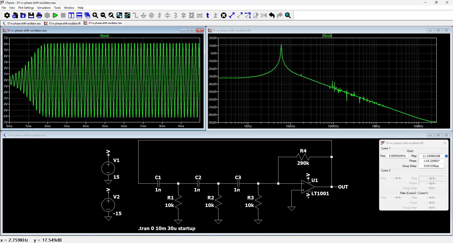
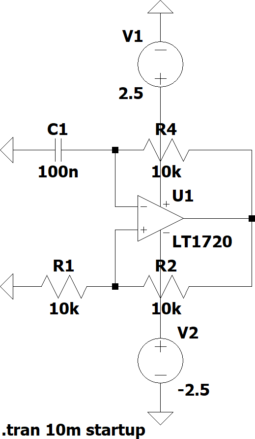
I start simulating the very first version of this circuit by Cătălina “Tank”:
On a first glance, nothing worth a fight. Seems to be a boring oscillator.
Next I found this mail of Andreas “Bullterrier”:
“Weird circuit… First, R3 should not have any effect. Second, why your frequency is shifted from the theoretical 6.5 kHz to 6.0 kHz ?”
First point seems rather sound…
A few mails later, this mail by Cătălina “Tank”:
“You stubborn! Simulations DOES show it has an effect.”
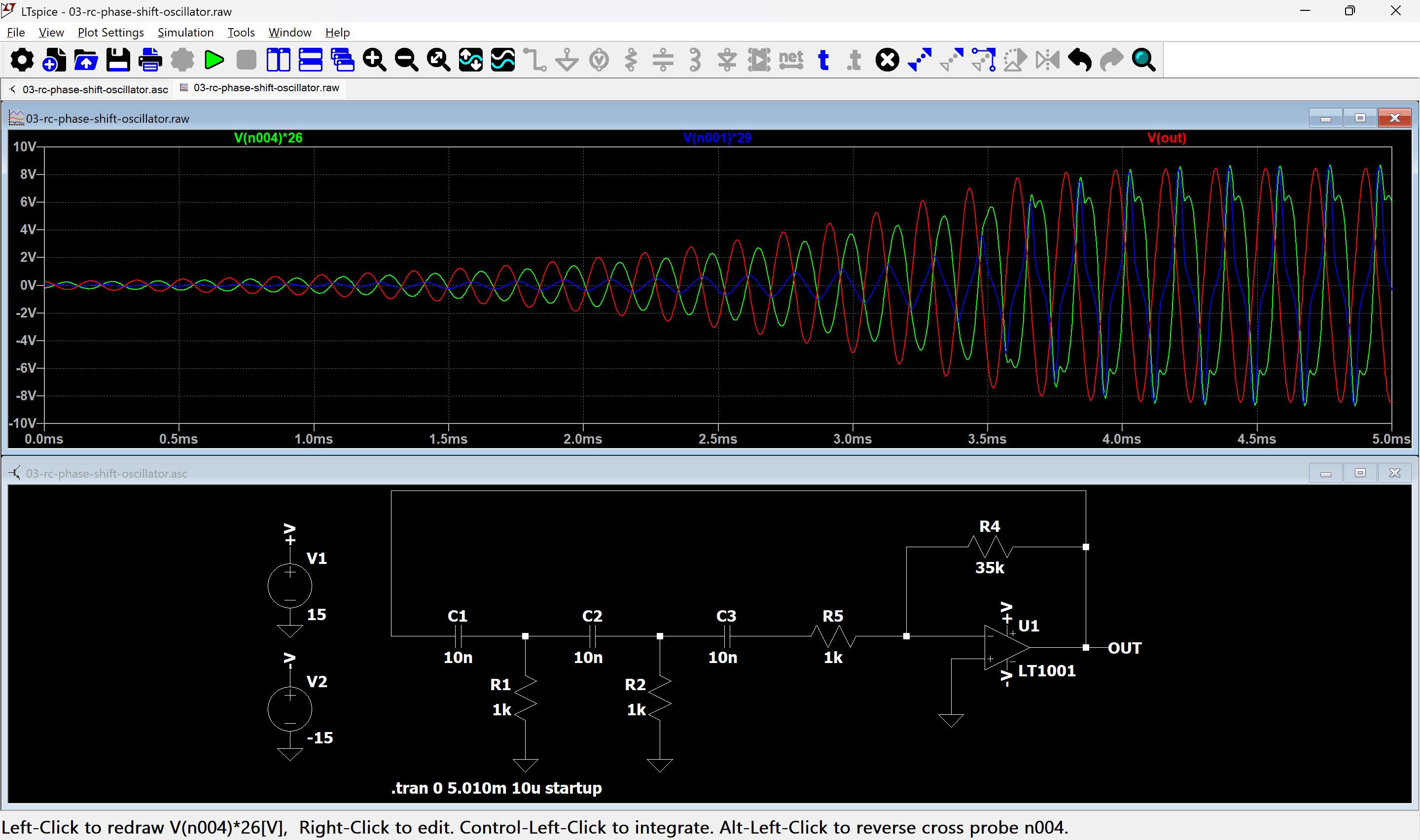
I was thinking this is typical from Cătălina when she lacks coffee… until I ran a simulation:
Holy damn. The resistor which should have no effect DOES HAVE an effect, and now the frequency is even further away from the theory: 4.5 kHz.
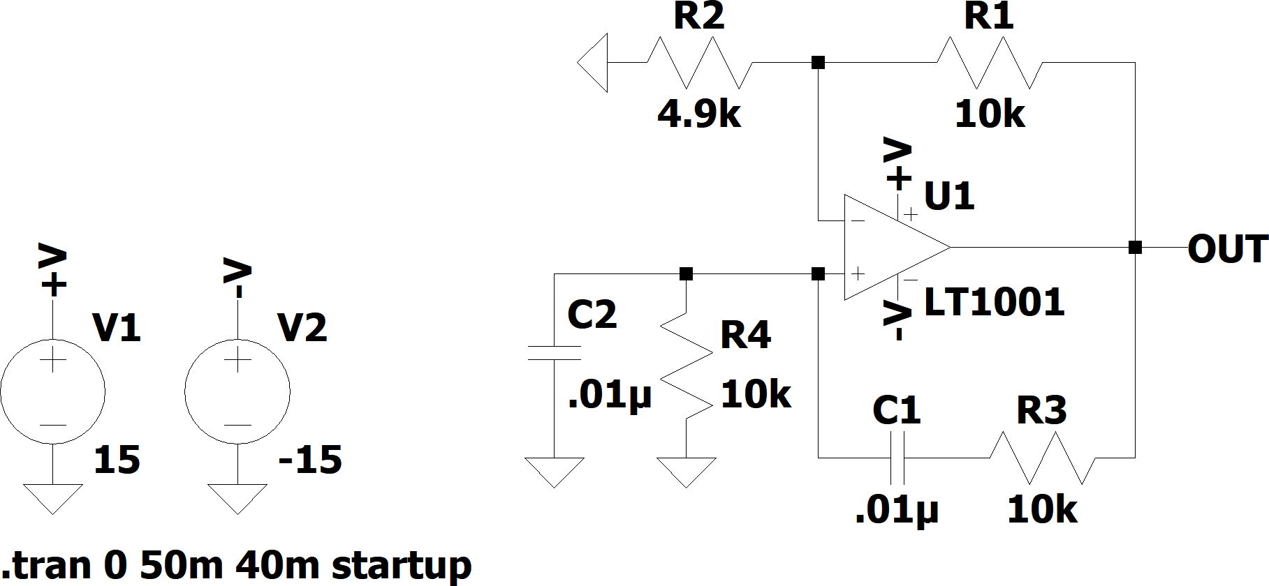
…even further
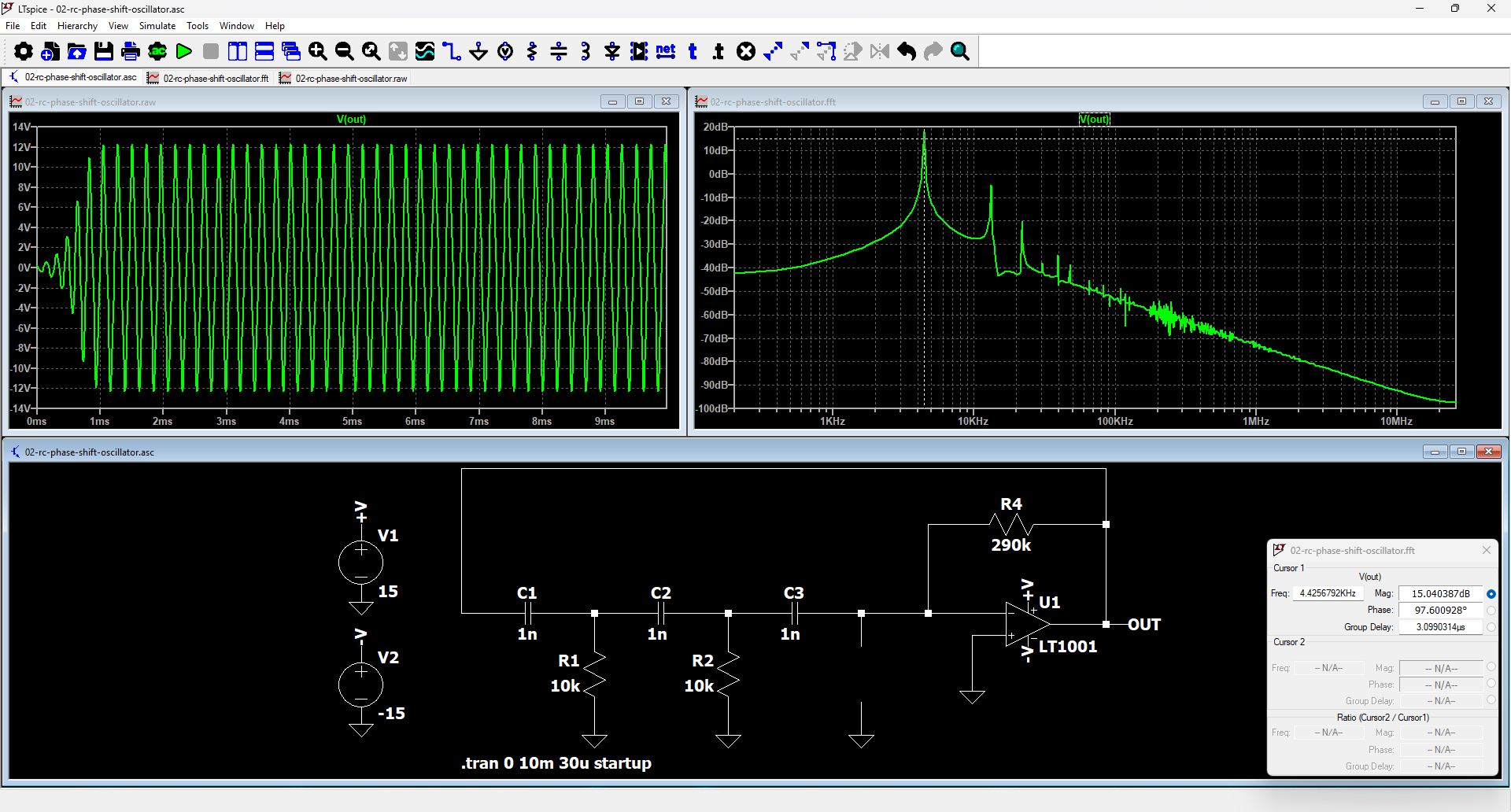
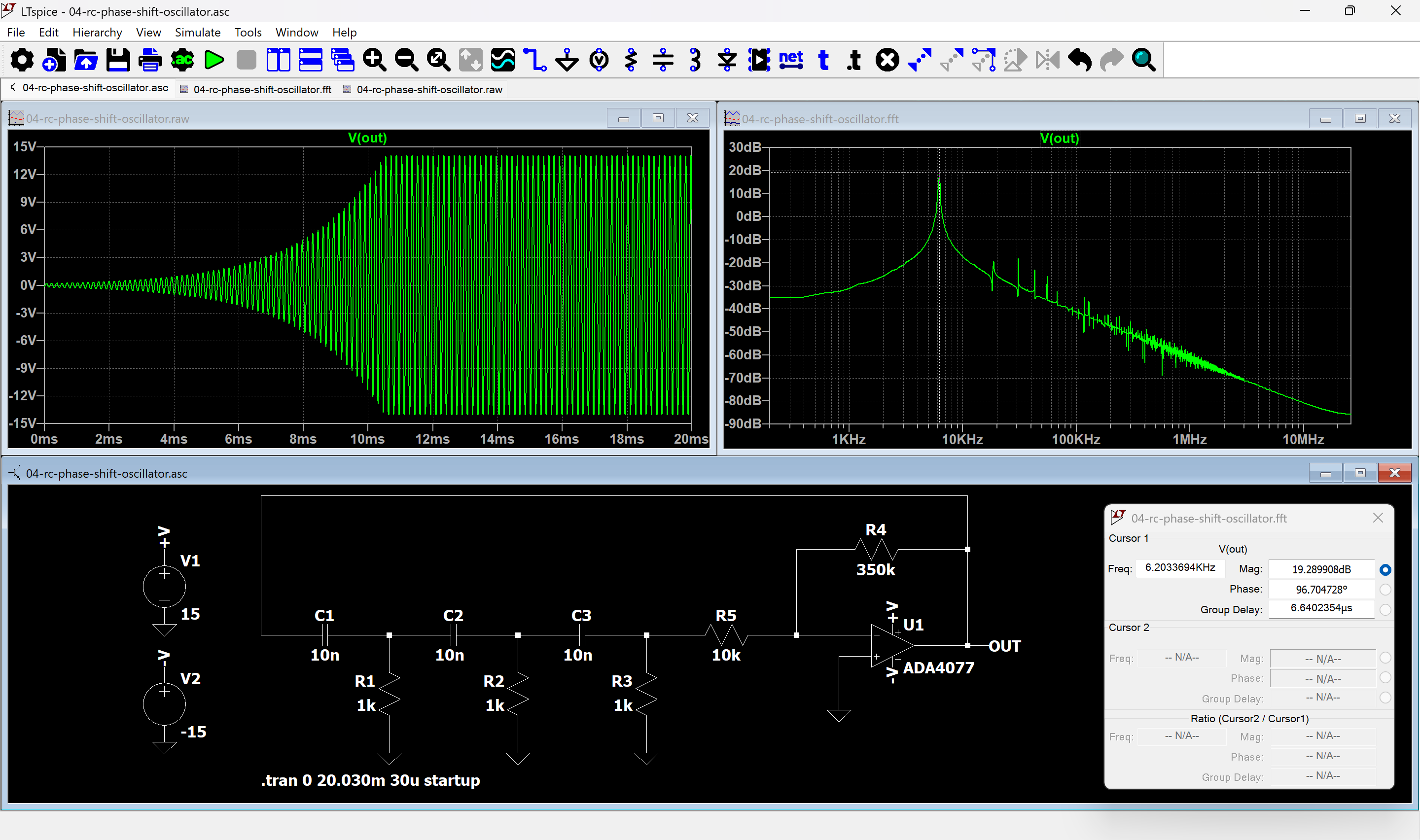
Next I simulate the first version proposed by Andreas “Bullterrier” which uses the input resistor of the inverting operational amplifier as an equivalent of the final shunt resistor:
The frequency is far from the theory, 5.0 kHz instead of 6.5 kHz, and the gain needed for a quick start higher than the theory.
Digging in the problem
All this stuff semm to have one question in common: what is actually the impedance of the operational amplifier circuit, no matter its variant.
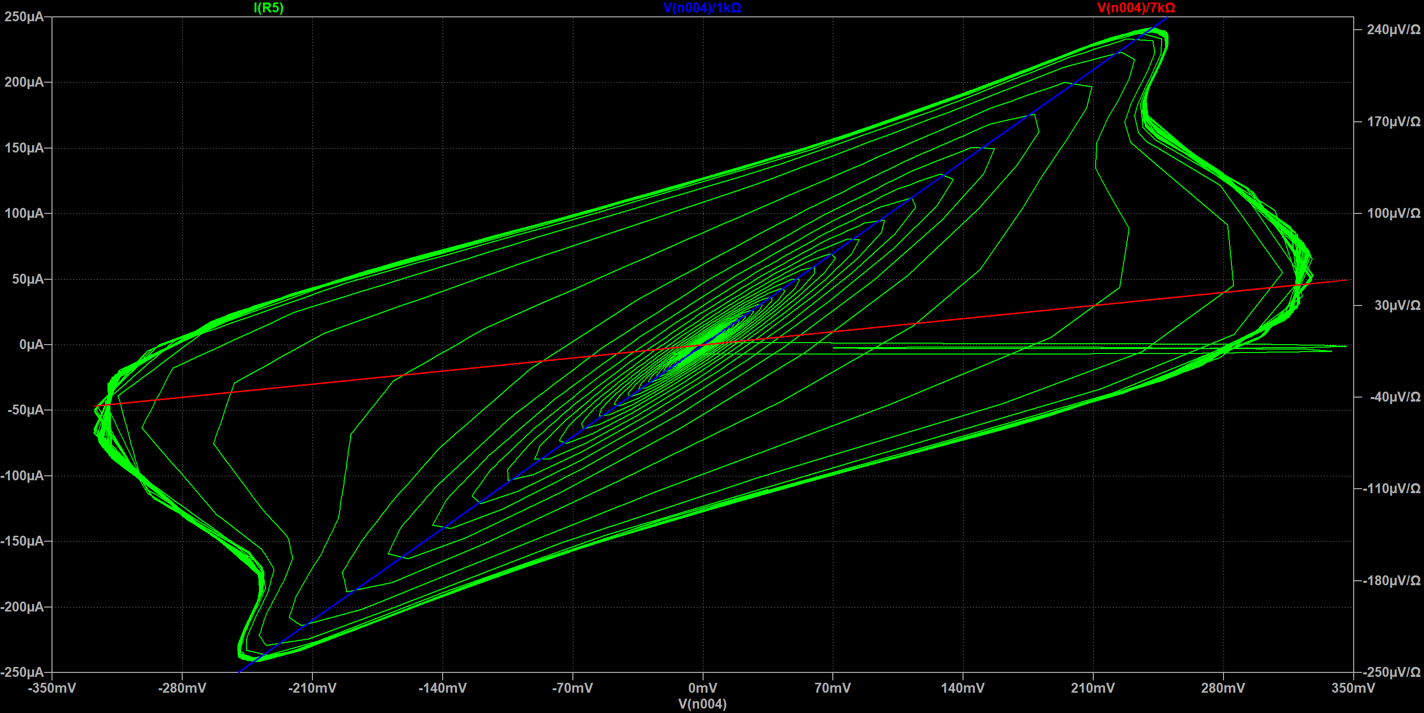
I made a Lissajous diagram to have a first look at the impedance:
We see that for low amplitudes the trajectory (green) is close to a 1 kΩ resistance (blue) but that for higher amplitudes the trajectory becomes much more complex, with a mixture of reactive behavior and of non-linearities for an equivalent impedance around 7 kΩ, much higher than expected at a first glance.
Andreas striked back
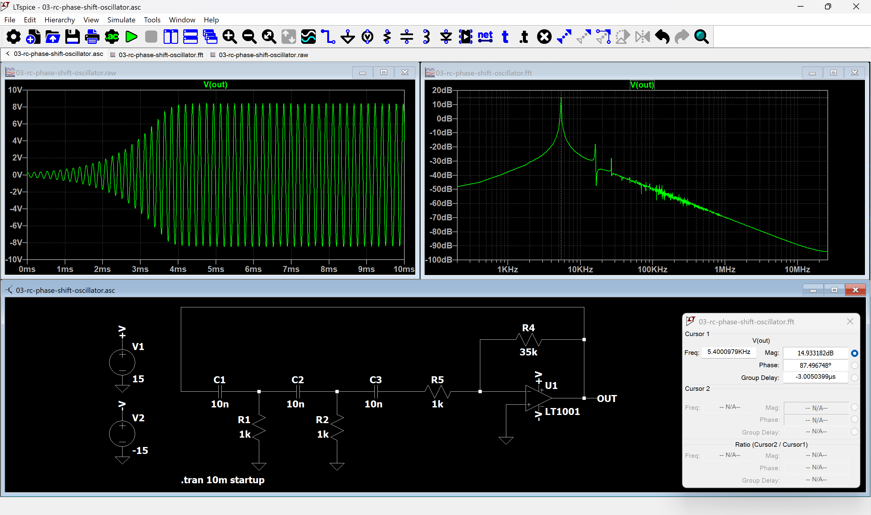
Andreas seems to have seen that the input impedance of the inverting amplifier what not the expected value since he made this second version I simulate:
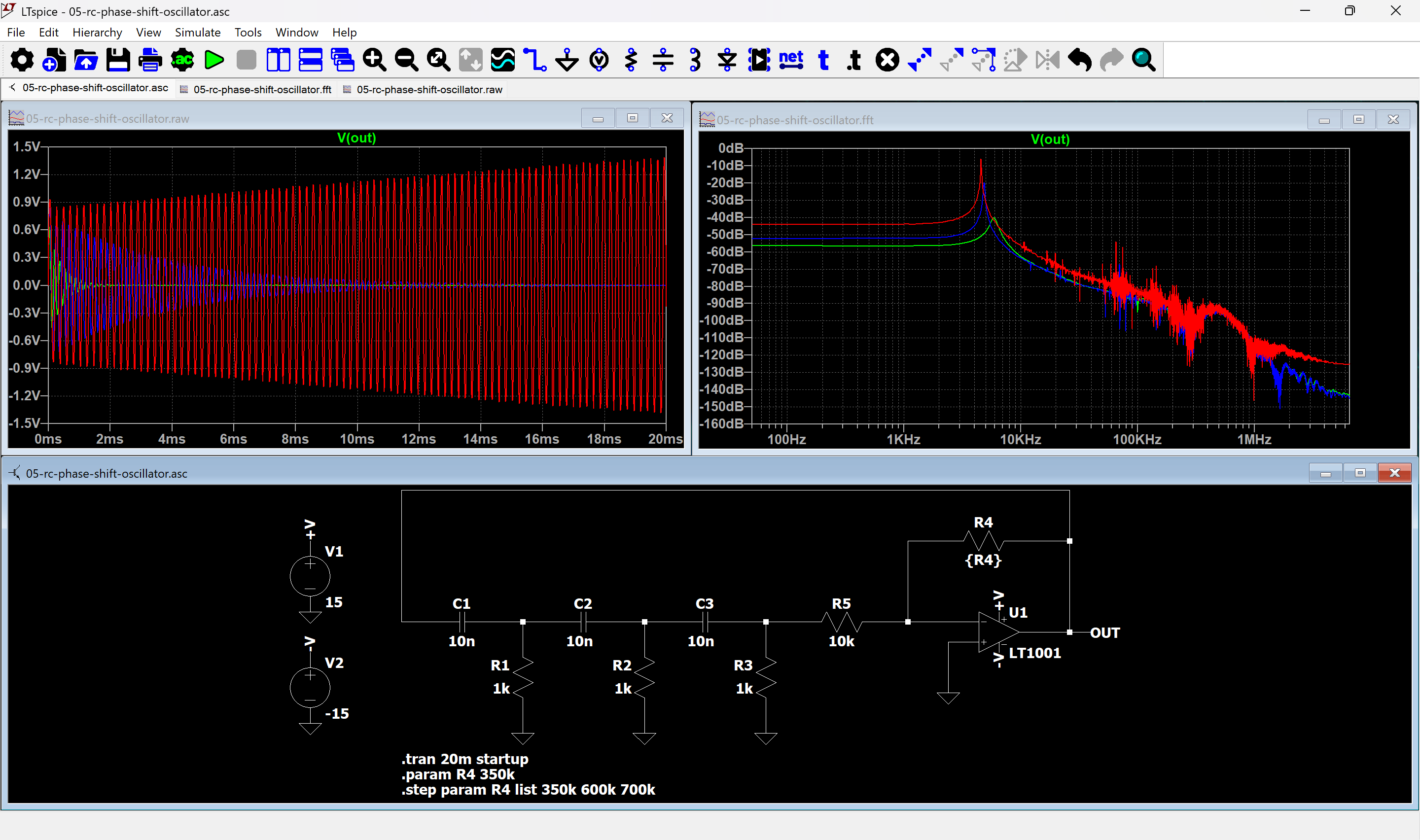
Indeed he used a shunt resistor and did not rely anymore on the input impedance of the operational amplifier. The oscillation frequency, 6.2 kHz, is closer to the expected value of 6.5 kHz. Again the needed gain is higher. But seems rather fine except…
Cătălina stikes back
"You ******* cheater. You made a comparison between circuits but changed the operational amplifier. Your damn **** does not work with the original amplifier while my circuit does."
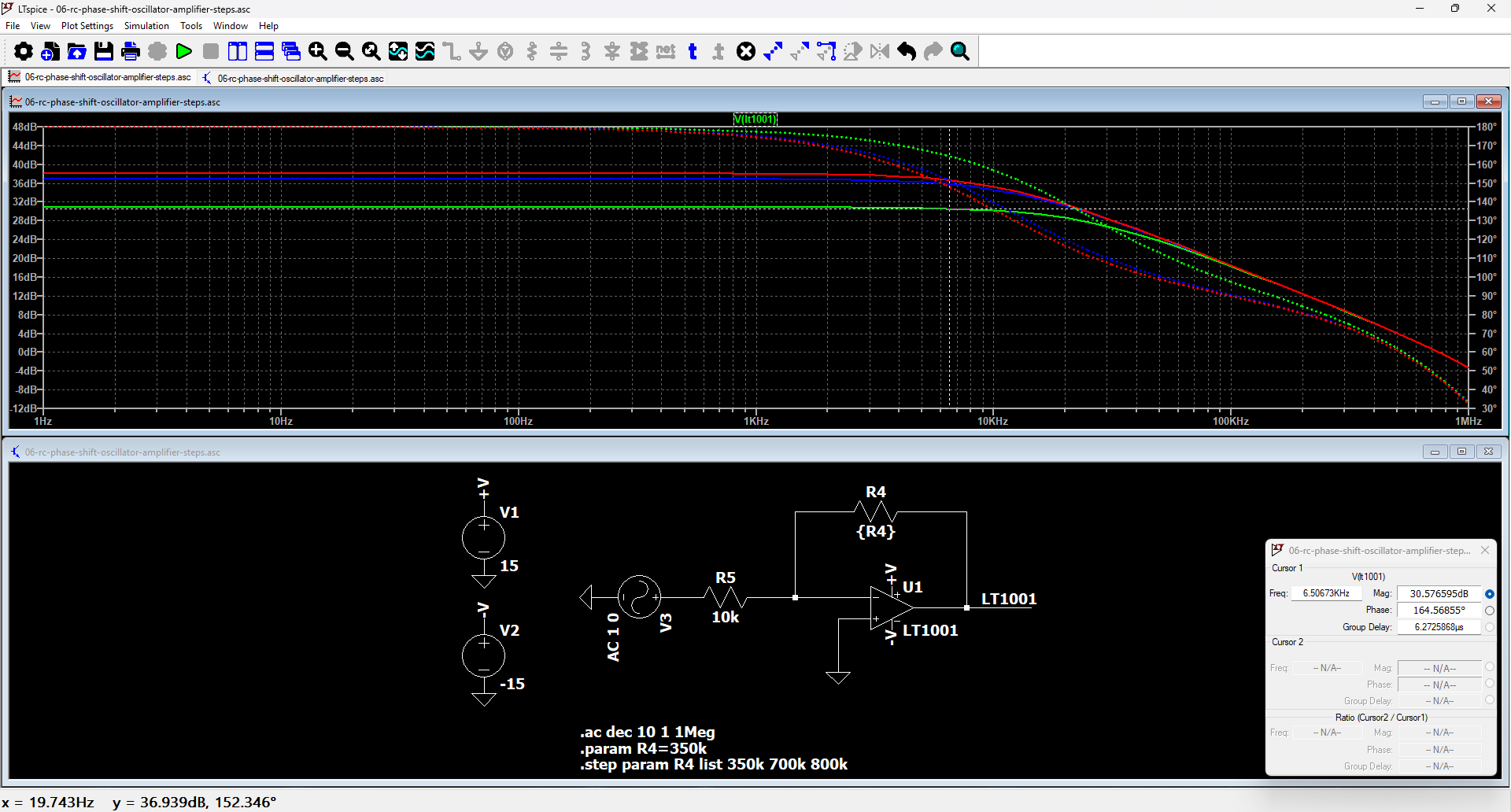
Indeed I missed this change. And when simulating with the original amplifier:
I need feedback amplifier gains much higher than the theoretical value, and the oscillation frequency, somewhere around 4.5 kHz was very far from the expected 6.5 kHz.
Digging
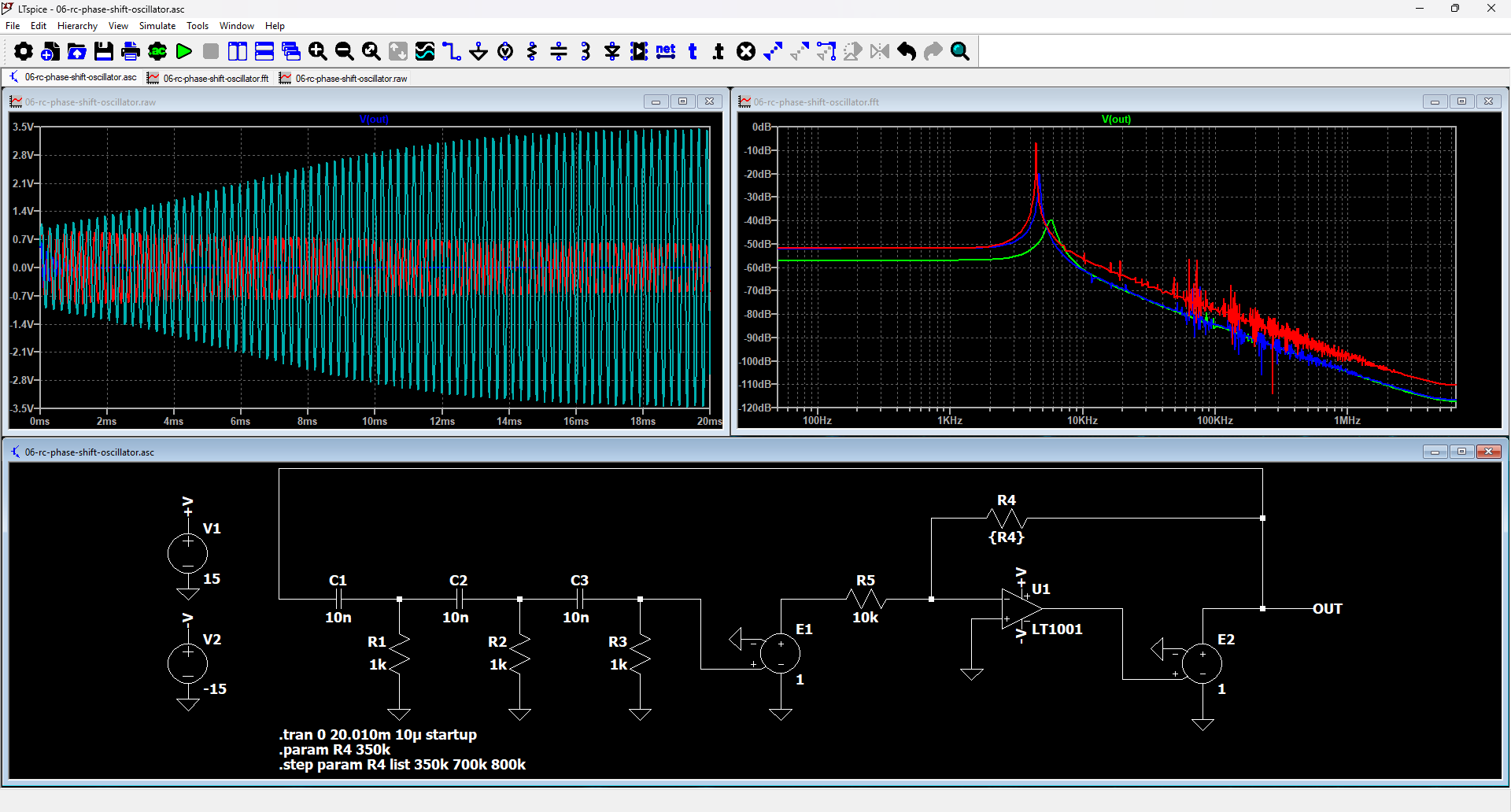
I tried first to check for any loading effects by introducing ideal followers before the RC and before the operational amplifier with its feedback:
Same tendencies, and the needed resistances are even worse. So, this problem is not in the impedances but really in the transfert functions. Since this problem depends on the operational amplifier, it is the point to check. And since it concerns also the low amplitude part, it should be seen also in small signal.
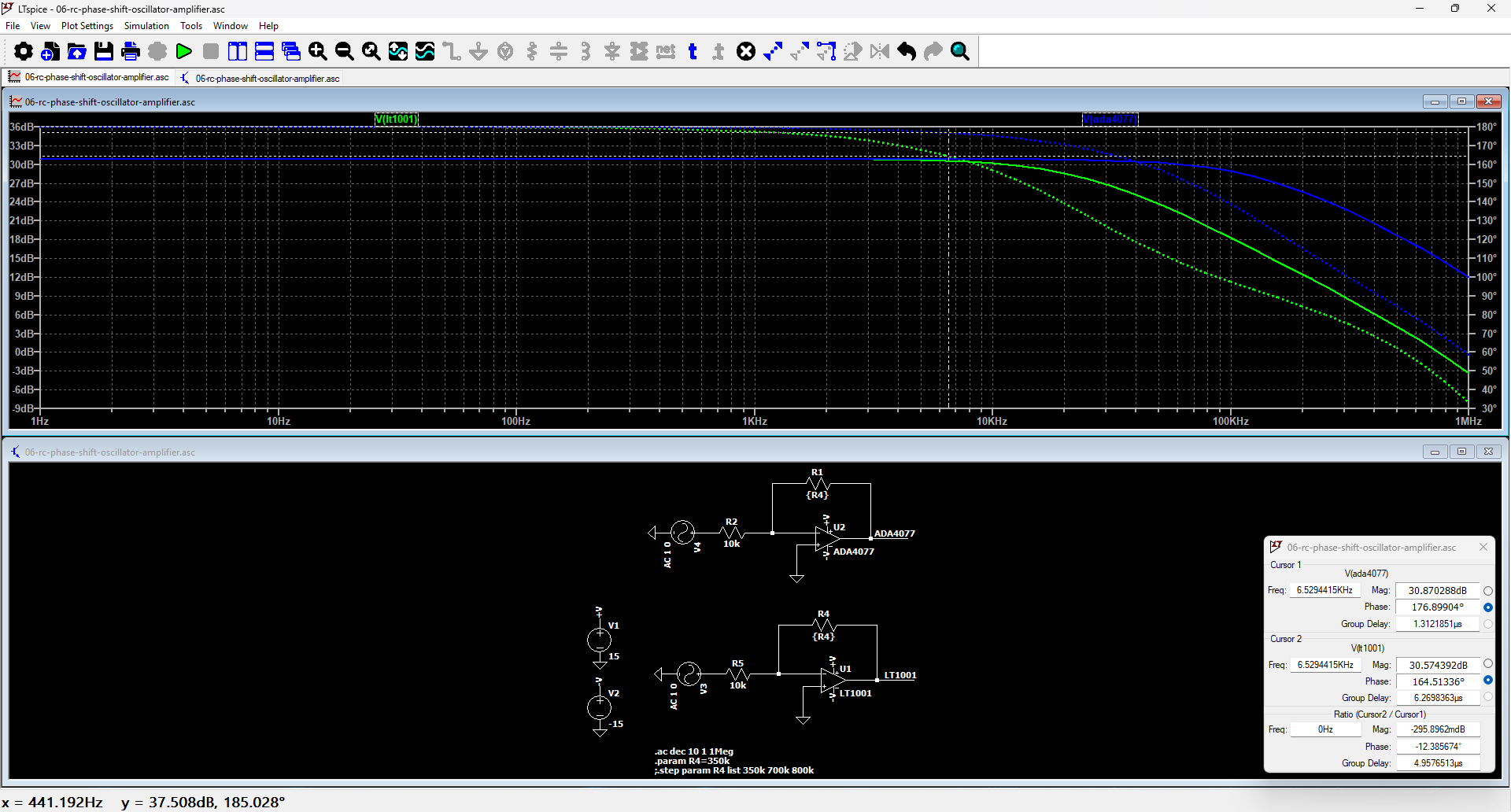
So I made a small signal simulation of the amplifying part with both operational amplifier models to compare:
The LT1001 has a low gain-bandwidth product, around 400 kHz in simulation, sufficient to provide the gain requested by the feedback, but with a 15.5° phase delay compared to the ideal value. On the contrary, the ADA4077 had only a 3.1° phase delay. Note the gain with both amplifiers is almost identical.
15.5° would not seem enough to wreak a circuit, but maybe RC phase shift oscillators are pricky ?
I begin to realize that this circuit might be monster and that it drove mad Andreas and Cătălina for a reason…
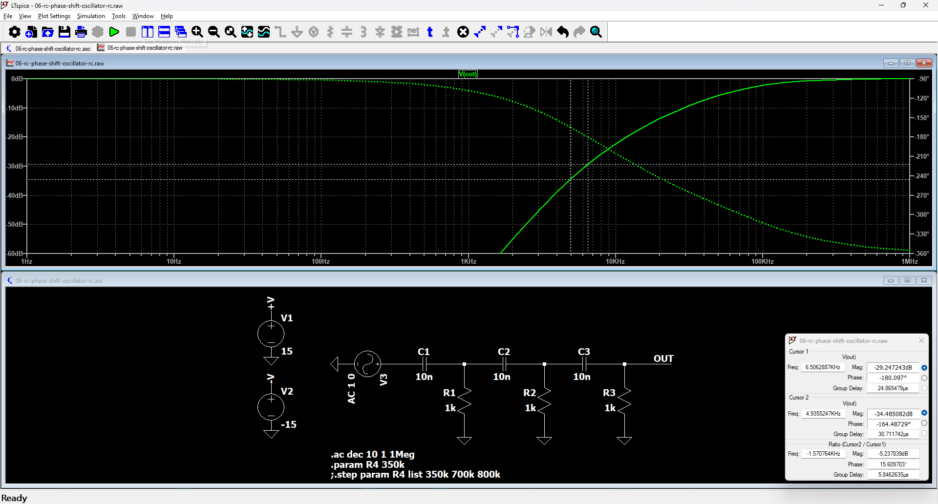
Next step is to simulate the RC network:
At the frequency shift needed to have a 15.5° phase advance to compensate the amplifier phase delay, a +5.2dB gain increase is needed to compensate the increased losses of the RC network. The value alone is not sufficient to explain the needed resistor values. However, when increasing the gain feedback resistor:
… the phase shift also increases, which increases again the losses of the RC network, which explains well the needed resistor values.
Straight to a solution
Enough of such falsely simple circuits. Lots of experimenters think they are simple because they manage to get something. But after how many hours of work ? And working reliably ? And at the correct frequency ? And so on. Making such oscillators is not as simple as it looks, and the story of Andreas and Cătălina is here to remind us this.
Time to enter in the 21th century.
The solution is simple and straightforward and is called direct digital synthesis (DDS):
Before detailing the subject, it is interesting to ask why using digital logic and digital to analog converters with their thoussands of integrated circuit transistors gets simpler than analog circuits with less than 20 integrated circuit transistors. The answer is in the question:
Because it leverages the specificities of integrated circuits.
The digital stuff and its thoussand of transistors can be easily integrated in integrated circuits, while the RC stuff is harder and takes lots of space. For instance, the compensation capacitor of the original 741 takes 1/3 of the chip according to Horowitz&Hill. The development is very costly, but can be reused in a much higher number of circuits than a particular RC oscillator.
Before the details, please take a break with a cat, courtesy of Wikipedia:
From a practical point of view, to use a DDS, you need:
A stable reference clock. But even the lowest cost crystal oscillator is better than RC oscillators. Advice: take an integrated stuff directly outputting a logic level clock. Making an oscillator from a crystal is not very hard, but don’t bring anything.
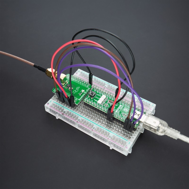
A DDS integrated circuit. Either bare or in a demo board which also integrates the quartz.
A microcontroller to set the DDS frequency. For this, use whatever you like. Also, the microcontroller is often already here.
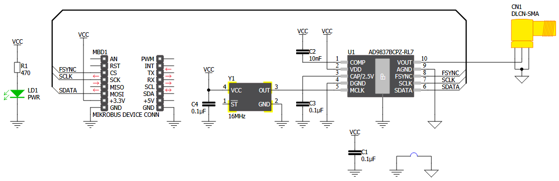
The schematic of the MIKROE waveform 3 click schematic, shown below, is self explanatory, except the dubious layout and grounding:
Greed LED and its resistor are mere convenience gadgets.
They used an integrated crystal like I advised.
And the DDS needs no other components than the decoupling capacitors.
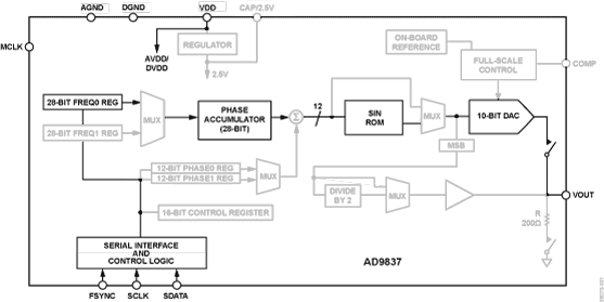
The schematif of the DDS itself, shown below, deserve more comments:
Parts not needed for understanding the base principle were lowered .
A synchronous serial interface allows to configure the chip. Particularly it allows to set the contents of a register containing the frequency. For each output sample, the phase of the output sinus is calculated by an addition. The phase accumulator overflows determine the signal period.
From this phase accumulator, an approximate sinus table is used to calculate the actual values of the samples. The two main sources of approximation are the truncature of the phase register, which determines the level of spurious, and the numbers of bits, which is the same as the ADC. After the sinus table, which converts the phase into a digital value, the digital to analog converter produces the actual voltage.
Other stuff in the schematic are:
A second frequency register to allow to easily commute between two frequencies.
A phase shift register to allow to easily commute between two phases of the signals. Note this register would not be very interesting if there were only one.
A control register to control the various parts (frequency and phase register selection, …).
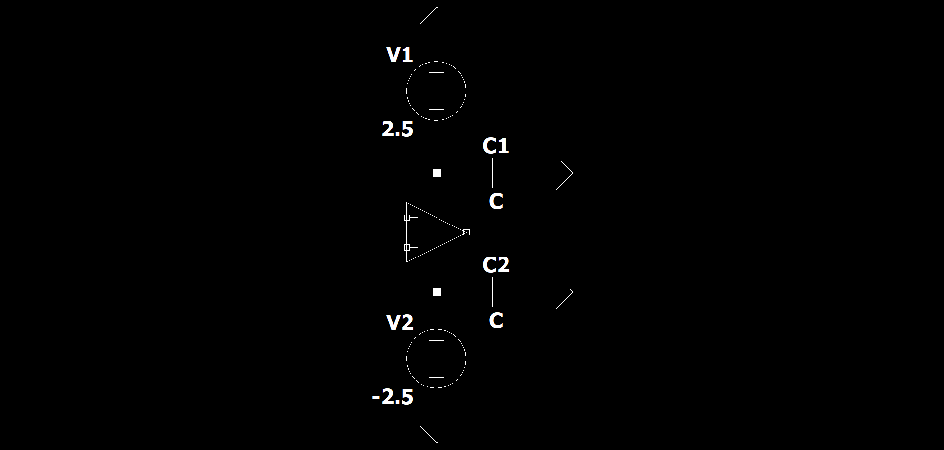
A 2.5V regulator to supply the inners of the chip and to avoid the user to do this itself.
A bypass of the sinus table to produce ramps.
A circuit to directly produce a divided clock instead of a sinus.
A circuit to control precisely the full scale amplitude of the digital to analog converter.
Now, time to write the report and to ask for payment in liters of coffee.
Epilogue
I received as a payment for this stuff approximately 50 liters of coffee, the standard currency in use at ACME labs.
The fancy oscillator stuff was dropped and replaced by very convenient DDS synthesizers.
Andreas and Cătălina have stopped their fight and promised to never touch damn circuits.
And on my side, still have a few cats to replace by more explanations, nothing new on the sun.
Appendix
A previous version of this article included some picture of a cat instead in waiting of the explanations to come. Please find it again:
After some discussions on grounding and various subjects with Gönül Demir, we thought that it could be a good idea to combine our both approaches to make a join page. Indeed I began my series by writing detailed articles about complex points and not by an introduction. We hope that this gentle (or not so) introduction to the topic would fill the gap.
What is an op-amp?
An operational amplifier (op-amp) is a high-gain analog amplifier designed to amplify the voltage difference between its two input terminals. Although the ideal op-amp model is considered simple, in practice op-amps have certain limitations and non-ideal behaviors. For this reason, op-amps are evaluated not on their own, but within a specific circuit context.
What is an op-amp used for?
In practice, op-amps are not used merely as “high-gain amplifiers”; they are mainly used to create controlled and predictable analog building blocks with the help of feedback. In this way, a single op-amp structure can perform many fundamental analog functions such as voltage amplification, buffering, summing–subtraction, active filtering, and providing impedance matching in measurement chains. In analog systems, the op-amp is a fundamental component that determines the amplitude and behavior of the signal.
Feedback
Negative feedback
Negative feedback was invented by Harold S. Black based on earlier works during his research on amplifiers for long distance analog telephony with multiple carriers multiplexing https://brewer.ece.gatech.edu/ece3043/FBBlack.pdf.
The gain of these tube amplifiers was not stable, which was troublesome because a wrong value of the gain compound with the multiple stages and lead to too low or too high outputs.
These amplifiers had also non-linearities issues which caused not only distortion of the individual carriers but also intermodulation between carriers.
Applying a negative feedback to an amplifier allow to trade a big gain against a stable gain. In the example given by Horowitz and Hill [2], an amplifier with a voltage open-loop gain varying from 1000 (60 dB) to 10000 (80 dB) end up with a 0.1 feedback (-10 dB) with a gain varying from 9.90 (19.91 dB) to 9.99 (19,99 dB), that is going from a +- 10 dB flatness to a +- 0.04 dB flatness.
This gain stabilization works no matter the root cause of the original gain variation. It works as well against changes in gain with time (thermal drift and aging), or changes in gain with frequency (dispersion), or changes in gain with amplitude (non-linearities).
Here, some beautiful cats instead of more complex maths.
Operational amplifiers and negative feedback
Operational amplifiers are explicitly designed to be used with feedback. However, an improperly applied feedback can cause circuits to oscillate, and indeed Harold S. Black had to solve instability issues.
Without diving too much in the theory , instability occurs when the loop gain is higher than 1 for a phase shift higher than 180°. Internal feedback is used in most op-amps so they behave approximately like integrators with 90° phase shift until their unity-gain bandwidth.
The integrator configuration is also convenient to have high gains at DC, and for most practical purposes the DC gain of an operational amplifier can be considered as infinite, and the operational amplifier as a pure integrator until its unity gain frequency, without the corner due to the finite DC gain.
Even if an integrator is not stable without a feedback look, integrators are very friendly for designers, even from a stability point of view, when used in a feedback loop. In addition, the internal feedback used to provide this integrator behavior pushes other poles further in frequency, due to a phenomena called “pole splitting”, so they don’t add too much phase before the unity gain frequency.
An operational amplifier is almost never used without negative feedback, at least because its high DC gain combined with its offset would make it saturate. A word of caution: a common mistake by beginners dealing with AC coupled signals is to forget the DC feedback.
Operational amplifiers and positive feedback
Although if less often used than negative feedback, the positive feedback is used typically for oscillators. Two configurations are worth mentioning: the Wien bridge oscillator and the RC feedback oscillator.
Wien bridge oscillator
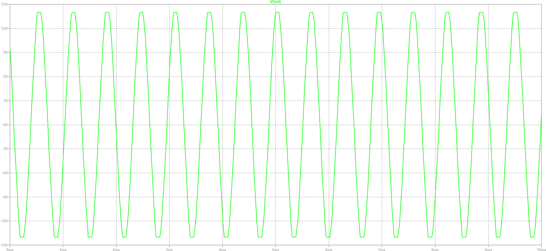
Simulation and output waveform of wien bridge oscillator without automatic gain control are shown below. Note the clipping of the waveform, which creates distorsion and harmonics. The root cause is that the loop gain must be equal to exactly 1 for sustained oscillation. Due to the tolerances of the various passives, the only way to get this condition exactly is to set the linear loop gain slightly higher than 1 and to count on the non-linear clipping of the amplifier to lower the actual non-linear loop gain to 1. This process creates distorsion and harmonics.
Schematic of a wien bridge oscillator without automatic gain control.Output after startup of a wien bridge oscillator without automatic gain control. Note the clipping of the waveforms.
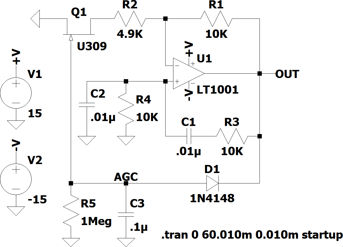
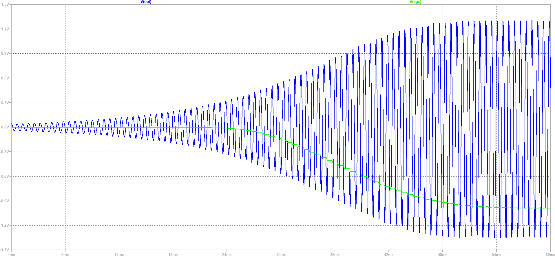
To avoid the drawbacks of the clipping method to set the loop gain, automatic gain control (AGC) can be used instead, like in the example below. The time constant of the exponential increase or decrease of the amplitudes of the oscillations is sufficienly high to allow setting the gain to the exact value of gain through a feedback look, called an automatic gain control. Note that the variation of the amplitude in function of the gain had a behavior similar to an integrator, so the unity gain can be reached for different amplitudes, and the gain is controlled indirectly through the amplitude. The plot show in blue the start of the oscillator with AGC and in green the output of the detector which, once below the threshold voltage of the JFET Q1, increases his resistance and lowers the gain set by the feedback loop R1 and R2+Q1.
Schematic of a wien bridge oscillator without automatic gain control.Output of a wien bridge oscillator with automatic gain control. The waveform has no clipping.
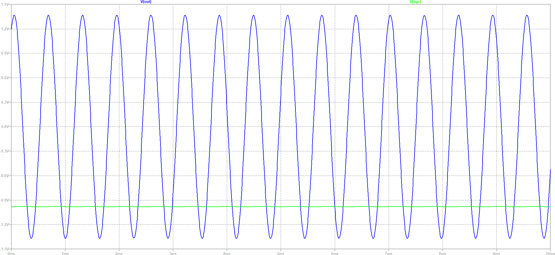
Details on the oscillations in etablished regime, shown below, show the absence of the clipping effect and the purity of the oscillations. The maximum timestep was reduced for easier plotting of the now beautiful shape of the waveform.
Simulation setup for etablished regime waveform details.Waveform details of a wien bridge oscillator with automatic gain control. No clipping is present.
We have also additional simulations for another article, stay in touch.
Comparators and positive feedback
With comparators, components used to compare two voltages and give a two state output (high or low), positive feedback is commonly used in the form of hysteresis for two reasons. 1/ Avoid multiple transitions in the case of noisy inputs. 2/ Decrease the output raise and fall times using the gain increase due to positive feedback.
However…… comparators are NOT operational amplifiers, and their use cases should not be mixed.
The following oscillator works in a comparator mode, which can be seen by the output taken discrete levels, and thus a comparator should be used for this schematic.
Schematic of an RC comparator oscillator circuit using positive feedback.Output waveform of the RC comparator oscillator showing discrete voltage levels characteristic of comparator operation.
Some sources on the internet use a 741 in this schematic. Don’t spread this mistake!
Op-amps according to input stage (BJT, JFET, MOSFET)
Operational amplifiers differ not only according to which application they are optimized for, but also according to the transistor technology used in the input stage.
This choice directly affects the op-amp’s input impedance, input bias current, and noise behavior. For this reason, it is a critical design parameter, especially in sensor interfaces and precision measurement circuits.
BJT-input op-amps
Thanks to their low input voltage noise and good matching characteristics, they provide an advantage when working with low-impedance sources.
In active-output sensors or low-impedance analog sources, noise performance is generally better.
On the other hand, since the input bias current is relatively high, they can lead to additional offset errors when used with high-impedance sources.
They provide much lower input bias current and high input impedance. With these characteristics, they are suitable for medium- and high-impedance sensors. Noise performance is generally weaker than that of BJT-input op-amps, but in practice the low bias current may be more important. In this respect, JFET-input op-amps are considered a balanced option between BJT and CMOS.
MOSFET (CMOS)-input op-amps
With extremely high input impedance and very low bias current, they are ideal for applications that require very high impedance and low power consumption.
Battery-powered systems and long-term DC measurements fall into this category. However, low-frequency noise (1/f noise) and temperature-dependent effects may be more pronounced; therefore, modern CMOS op-amps are often supported with zero-drift architecture.
A simplified schematic of a typical CMOS operational amplifier is shown below:
Simplified schematic of a typical CMOS operational amplifier input stage from the OPA391 datasheet (https://www.ti.com/product/OPA391).
In summary, if the source impedance is low, a BJT input is preferred; for medium-to-high impedance sources, a JFET input; and for very high impedance and low power requirements, a CMOS input is generally the most suitable choice.
This distinction plays a decisive role in measurement accuracy and system stability, regardless of the op-amp type.
Op-amp types according to application and performance purpose
Operational amplifiers do not consist of a single structure; they are designed by prioritizing specific characteristics in line with different application requirements
For this reason, op-amp types are classified not by how they operate, but by the intended use for which they are optimized.
This classification constitutes the first and most important elimination step when selecting the correct component
General-purpose op-amps
They offer balanced performance among bandwidth, noise, offset, and power consumption.
They are widely used in education, prototyping, and non-critical analog circuits. In most designs, the first op-amps tested belong to this group.
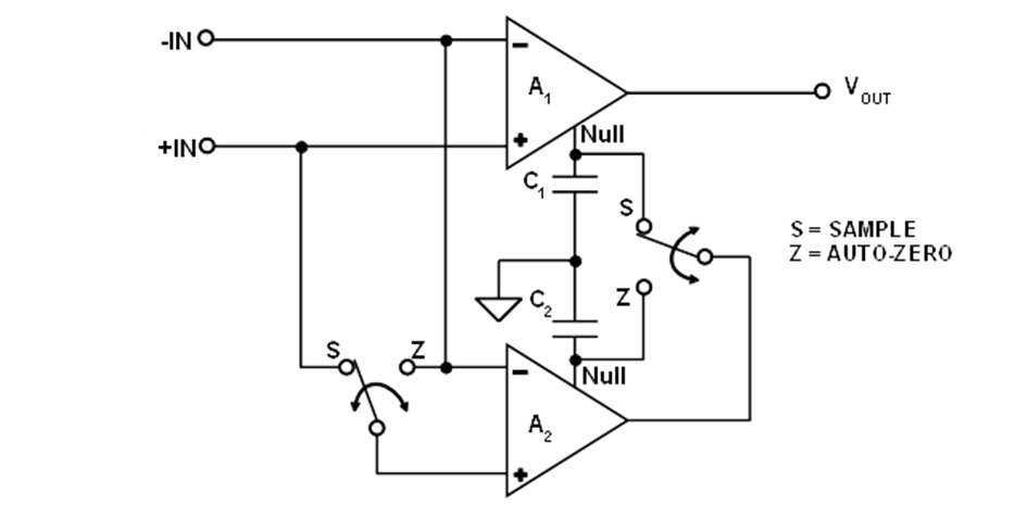
Precision op-amps
They are designed for applications where DC accuracy is important, with low input offset voltage and low temperature drift.
Sensor interfaces, current measurement circuits, and front-end stages of high-resolution ADCs are typical application areas for this class.
High bandwidth is generally not a priority in these op-amps.
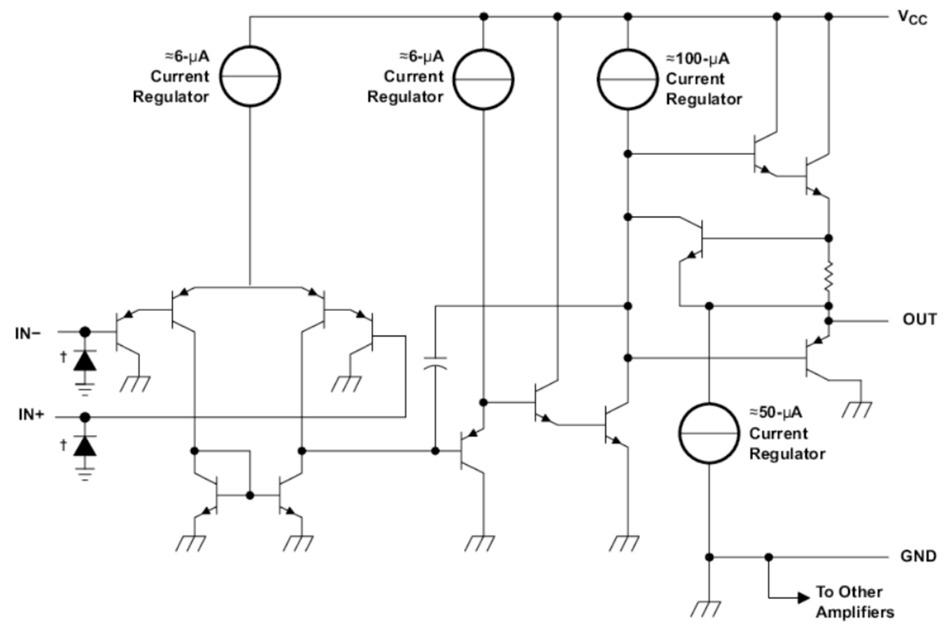
Block diagram of an auto-zero operational amplifier showing the two amplifier stages and switching mechanism.
They use internally two amplifiers and alternate between two modes:
The correcting amplifier zeros itself by connecting their inputs together and adjusting its own compensation capacitor to compensate its own offset until it sees a zero at its input
The correcting amplifier zeros the corrected amplifier by adjusting the compensation capacitor of the corrected amplifier to compensate its offset until it sees a zero at its input.
With this technique, offset and drift is reduced to very low values.
Usually, bipolar amplifiers are preferred when searching for low offsets. However, auto-zero amplifiers are often CMOS amplifiers because switches are much easier to realize in CMOS.
While they provide a maor advantage in measurement systems where DC accurary (offset) and long-term stability (offset drive) are critical, they exhibit switching noise and can also have more subtle issues, like recovery from overload (the correcting amplifiers trying to compensate the input difference even if it is not due to an offset). Pay attention to the datasheet.
Audio op-amps
They are optimized for low distortion (deviation of the signal from the ideal waveform) and highly linear behavior within the human hearing band.
Total harmonic distortion (THD) (the ratio of harmonic frequency components present in the output signal that are not present at the input), output drive capability, and linearity are prioritized; absolute DC accuracy is often of secondary importance.
They are preferred in audio signal chains.
High-speed op-amps
They are developed for applications requiring wide bandwidth and high slew rate. Video signals, fast data acquisition systems, and high-frequency analog processing fall into this category.
These op-amps are more sensitive to layout, feedback network design, and stability issues.
Current-feedback amplifiers (CFA)
They use a different architecture from voltage-feedback op-amps.
While voltage-feedback amplifiers have their output depending on the difference between the voltages at their inputs, current feedback amplifier apply on their IN- terminal the voltage they get on their IN+ input and have their output depending on the current flowing in the IN- input.
Voltage feedback amplifiers are usually compensated to be stable when used as unity gain followers, a more difficult situation for stability than amplifiers having a gain higher than unity, since the feedback for unity gain is higher. When such amplifiers ar used for higher gains, they are clearly over-compensated, which reduced their performance.
On the contrary, with current feedback amplifiers, compensation is adjusted using the feedback resistor, so it has the right value when using higher gains.
This is one of the reason they are very popular, and also why this feedback resistor must have the value recommended by the manufacturer.
The need of a rather low feedback resistance seems inconvenient, but current feedback amplifiers are almost always used for high-speed design where voltage feedback amplifiers would also need a low feedback resistances to avoid the effects of input capacitances. Indeed, in some circuits, both families are in practice almost interchangeable.
For instance, the differential amplifier which gave me the opportunity to write this note (/posts/diff-amp-equations.html), used actually an ADA4927 which is a current feedback amplifier, but for some reason the demo circuit used in the webpage uses an ADA4937 which is a voltage feedback amplifier. But this works well because:
both have the same footprints, even if not relevant for an LTSpice simulation,
the recommended feedback resistor value for the current feedback amplifiers are often in the range of recommanded values of high-speed voltage amplifiers, and
feedback allows to have a similar circuit work with both types: input current or voltage is low enough for calculations.
The feedback must be resistive, at least the resistive part of it must be dominant. Never directly a capacitor as a feed back.
Slew rates are also faster than voltage-feedback op-amps. In voltage-feedback amplifiers, the output current of the first stage is limited by the current source which in combination with the compensation capacitor limits the slew rage. On the contrary, in current-feedback ampflifiers, this current is directly fed by the user. More details can be found in https://www.analog.com/en/resources/analog-dialogue/articles/current-feedback-amplifiers-1.html .
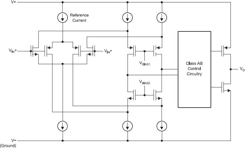
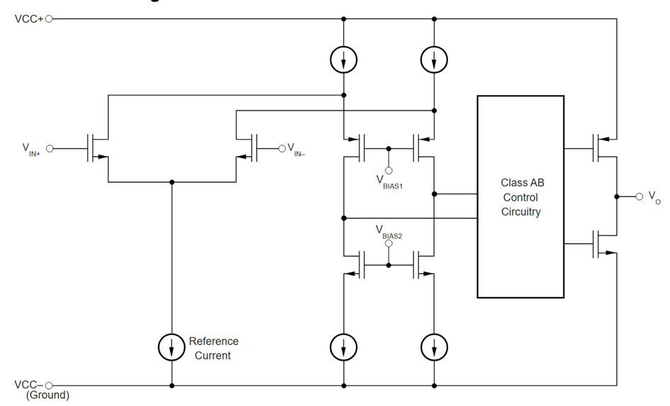
Op-amp input stage headroom according to structure
This one is often overlooked but pay attention to this. With some training, it is possible to see at a first glance on the equivalent schematics an idea of the inputs headrooms.
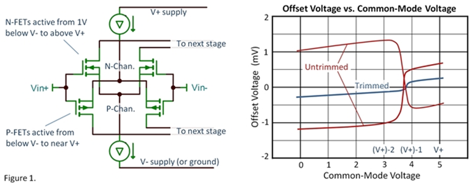
Simplified schematic of the TL081 operational amplifier showing N-channel JFET input stage.
Both transistors are source followers trying to apply to their source their input minus some voltage. Guess something between 1 V and 2 V. The current source needs also some headroom. On the other side, there is not so much constraint between the input and the drain.
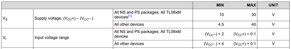
So, the input range can be inferred as: V- + headroom to Vcc. And indeed the datasheet:
TL081 datasheet specification showing input voltage range extending from ground + headroom to slightly above Vcc.
Input range: ground + headrom to slightly higher than Vcc.
P input stage
Simplified schematic showing P-channel input stage configuration with input range from slightly below ground to Vcc - headroom.
Input range: slightly lower than ground to Vcc – headroom.
Op-amp parameters describe the extent to which the amplifier deviates from ideal behavior.
None of these parameters is “good” or “bad” on its own; what matters is which one is decisive for a given application
Availability
Cost, distributors, delays, MOQ, …
Convenience stuff
Packages, …
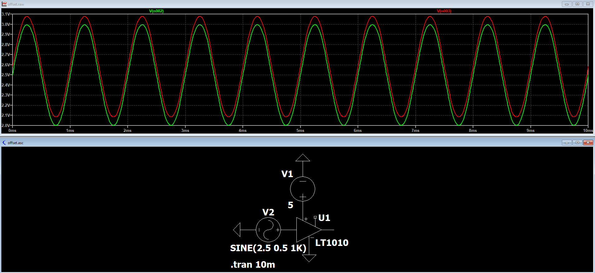
(Input) offset Voltage
It is the small differential input voltage required for the output to be exactly zero when the op-amp inputs are theoretically at the same voltage.
In other words, it is a DC error arising from the op-amp’s internal imbalance.
Simulation schematic and output waveform of a LT1010 buffer with input offset voltage.
Applications for which this parameter is critical
Low-level DC measurements.
Sensor interfaces.
Current sensing.
Bridge circuits.
Applications for which this parameter is secondary
AC-coupled circuits.
Audio signal processing.
High-amplitude signals.
Disadvantages of good values
Very low offset generally implies a more complex internal architecture and higher cost.
Input (dynamic) resistance
The input (dynamic) resistance of an operational amplifier circuit should be high enough compared to the output impedance of the signal source to avoid loading it.
In inverting or substracting amplifiers, this input resistance is determined mostly by the resistors of the network, which must be carefully selected: not too big to avoid loading the signal source and not too high to avoid noise and issues with parasitic capacitances.
When the signal source is directly connected at the input of an operational amplifier, the impedance it sees it directly determined by the operational amplifier input impedance, so it is an important parameter to check in these cases with an high-impedance source.
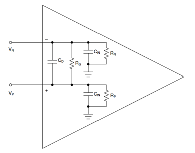
Operational amplifier input resistance model showing differential (Rd) and common-mode (Rn, Rp) components.
Datasheets give the elements between the inputs and the elements to ground in different ways.
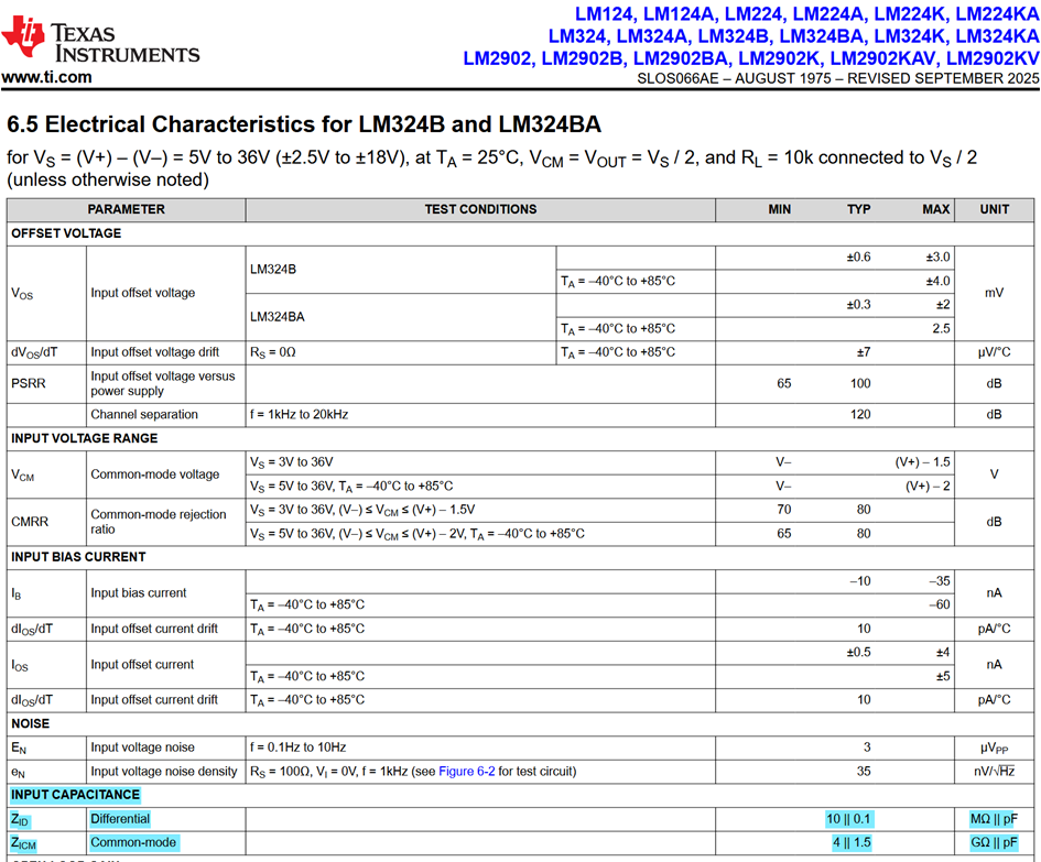
In the LM324 datasheet (https://www.ti.com/lit/ds/symlink/lm324.pdf), the differential-mode input resistance rid = Rd || (Rn + Rp) and the common-mode ric = Rp || Rn are given:
The common mode resistance is 400 times higher than the differential due to the operation of the input stage, which is a common behaviour.
The common-mode is indeed much higher than the differential mode.
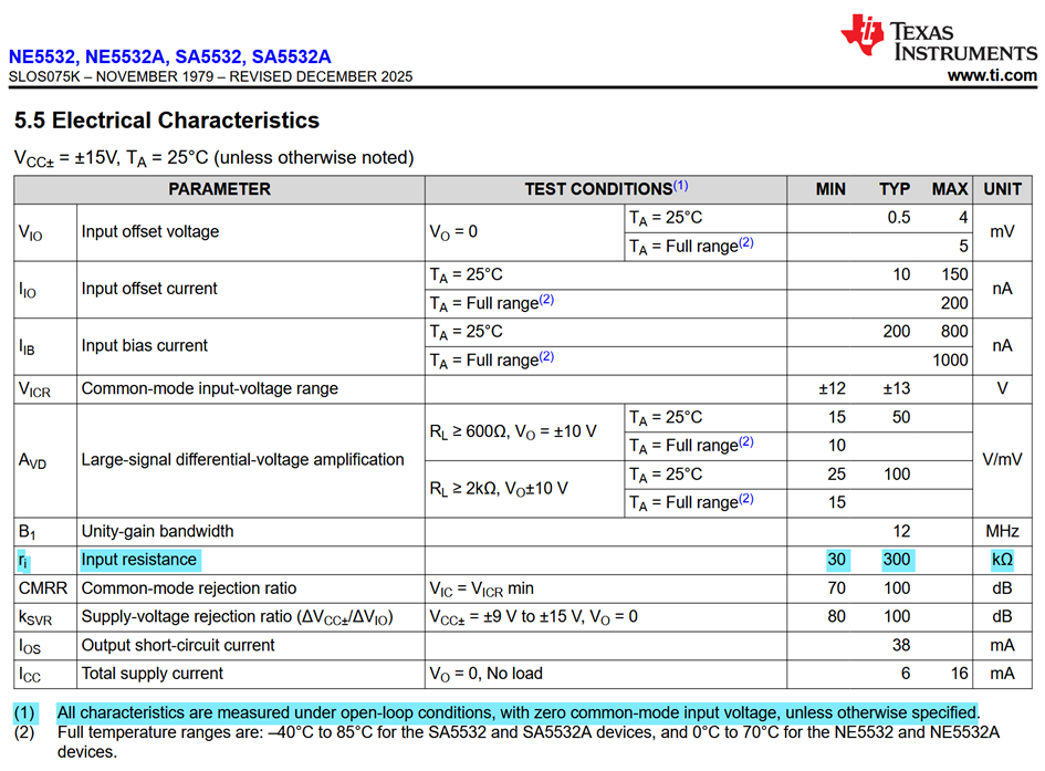
In the NE5532 datasheet (https://www.ti.com/lit/ds/symlink/ne5532.pdf), the impedance of one input when the other is tied to ground, called single-ended in the jargon, ri = Rd || Rn is given:
NE5532 datasheet specification for single-ended input resistance (ri) measurement configuration.
No information is given on the common-mode, but is can be reasonably guessed for most purposes that ri ≈ Rd and that Rp and Rn are much higher than Rd.
Due to feedback, the effective input resistance will be higher, but this is still a low value for an op-amp. This is because this operational amplifier is optimized for low-noise.
Most often this value is a check of being in the right ballpark for the use rather than a precise calculation. Here, this amplified is clearly suited only for low input impedances.
When this parameter is important, for DC or near DC, pay attention also to the bias current, and for higher frequencies, pay attention also to the capacitances. For the values of the LM324, the common-mode capacitance starts to dominate the differential-mode resistance from only 11 kHz.
Advantages of high input resistance
The signal source is not loaded
The measured voltage is transferred to the op-amp without distortion
High-impedance sensors (e.g., thermistors, piezo elements, electrodes) can be read correctly
Disadvantages of high input resistance
Higher 1/f noise is generally observed in MOSFET/CMOS inputs
Beware of
Bias currents
Capacitances
Static electricity (whole circuit, not just the op-amp, often including ESD protection)
Leakage currents (rather due to the need for high impedance than due to the op-amp)
PCB contamination and humidity (idem)
(Input) offset drift
Input offset drive belong to two main categories: thermal drift, depending on temperature, and time drift, which is a longer term aging.
Thermal drive is typically specified in µV/°C.
Time drift is often specified in µV/month or µV/1000 hours. However, these units can be misleading. Since aging is a random walk (“drunkard’s walk”) phenomenon, it is proportional to the square root of the elapsed time https://www.analog.com/media/en/training-seminars/tutorials/MT-037.pdf and 1 µV/1000 hour actually corresponds to 3 µV/year instead of 9 µV/year.
Applications for which this parameter is critical
Long-term measurements.
Industrial and field systems operating over a wide temperature range.
Applications for which this parameter is of secondary importance
Short-term systems with stable temperature.
Disadvantage
Very low drift often requires zero-drift or chopper architecture, which can generate additional low-frequency noise.
Input Bias Current
It is the small DC current that flows from the inputs to enable the operation of the op-amp’s input transistors.
Applications for which this parameter is critical
High-impedance sensors.
Piezoelectric elements.
Circuits operating with large-value resistors.
Applications for which this parameter is of secondary importance
Low-impedance sources (e.g., <1 kΩ).
Disadvantages of good parameter values
Very low bias current is usually achieved with MOSFET/JFET inputs, which in some cases leads to higher 1/f noise.
CMRR (common-mode rejection ratio)
The CMRR of an amplifier circuit is the ratio between its differential-mode gain and its common-mode gain, expressing its ability to extract a small differential signal superposed to a big common-mode signal.
Before even looking at the datasheet, it should be emphasized that bit factor in the CMRR (or the lack of) is the topology of the circuit and the mismatch of the resistors. Most operational amplifiers have CMRR higher than 70 dB while common resistors are closer to 1 % tolerance. Solutions exists to overcome this point, like the classical 3 operational amplifier differential amplifier, but must be studied carefully before even having a look on the CMRR number of the datasheet.
Applications for which this parameter is critical
Differential measurements.
Current sensing.
Noisy industrial environments.
Applications for which this parameter is of secondary importance
In practice, CMRR depends not only on the op-amp but also on the matching of external resistors. The datasheet value cannot always be achieved in the system.
PSRR (power supply rejection ratio)
The power supply rejection ratio (PSRR) is the ratio of the variations of the input/output of an operational amplifier relative to the variation of their power supplies.
According to https://www.analog.com/media/en/training-seminars/tutorials/MT-043.pdf which gives lots of valuable explanations on this topic, this quantity should named PSRR when expressed in linear units, and PSR when expressed in dB, but nobody seems to follows exactly this convention.
So, in doubt, assume worst case for your circuit between input and outpout.
PSRR can be measured and specified either for the positive supply, either for the negative supply, or for a symmetrical change in both supply. The latter case is often seen but not realistic, because noise on both supplies is likely to be different. In this last case, since the middle of both supplies is likely to move also, not only the “symmetrical PSRR” but also the CMRR must be taken into account for a detailed calculation. Anyway, both quantities have similar origins and similar values.
Applications where this parameter is critical
Battery-powered switching power supplies, typically used with low voltage batteries or when multiple voltages are needed.
Noisy supply rails, either due to the supply of due to the loads.
Applications where this parameter is of secondary importance
Well-regulated, low-noise laboratory power supplies.
Disadvantage of good parameter values
High PSRR generally requires a more complex internal circuit structure.
Gain–bandwidth product (GBW)
It defines the fundamental limit between gain and frequency of the op-amp; as gain increases, the usable bandwidth decreases.
Applications where this parameter is critical
Wideband signals.
Fast control loops.
Video and high-speed analog processing.
Applications where this parameter is of secondary importance
Slowly varying DC measurements.
Disadvantage of good parameter values
Unnecessarily high GBW can lead to excess noise and stability problems.
Slew rate
It is the maximum rate at which the output voltage can change over time (V/µs).
Applications where this parameter is critical
High-frequency or high-amplitude signals.
Applications where this parameter is of secondary importance
Low-frequency and slowly varying signals.
Disadvantage of good parameter values
High slew rate often comes with higher power consumption.
Illustration of slew rate limitation showing how finite slew rate causes waveform distortion in high-frequency signals.
Noise consists of unwanted random signal components generated internally by the op-amp; it includes wideband noise and low-frequency 1/f noise .
Applications where this parameter is critical
Low-level signals.
High-impedance sources.
Precision measurements.
Applications where this parameter is of secondary importance
High-amplitude or digitally dominated systems.
Disadvantage of good parameter values
Low noise is often achieved at the expense of power consumption or bandwidth.
Headroom
Headroom expresses how close the op-amp inputs and outputs can approach the supply rails.
Applications where this parameter is critical
Single low-voltage supply with non–rail-to-rail amplifiers; insufficient headroom leads to signal clipping and loss of linear behavior.
Applications where this parameter is of seconrady importance
Wide dual-supply (±12 V, ±15 V) circuits operating far from the rails.
Summary
Op-amp selection is not about making all parameters “the best”.
Correct design means prioritizing the parameters that are critical for the application and keeping the others at a sufficient level.
References: [1], [2], [3], [6]
Op-amps according to output types
The output stage of an op-amp determines how the amplified signal is presented, with respect to which reference it is defined, and which loads it can drive.
Although often overlooked, the output type directly affects design success, especially at low supply voltages, when driving ADCs, and in digital–analog interfaces.
Single-ended vs. fully differential output
Most operational amplifies have a single signal output, configuration called “single-ended output”. This output is often referred to the ground. While amplifiers used with a single supply are connected to this ground and to the positive supply, amplifiers used with a dual supply are connected to the negative and to the positive supply voltages, but almost never directly to the ground.
So, and particularly in cases where the supply voltages move for whatever reason like noise, which is the reference actually used by the operational amplifier ?
Turns out that this question depends a lot on the internal structure, can even be different between input and output stages, and even depends on the common-mode input voltage and output voltage for rail-to-rail operational amplifiers.
So, for pratical purposesn, the reference can be considered as being the ground, the power supplies must be decoupled to it, and the PSRR (see section power supply rejection ratio) must be checked because this ratio will precisely tell to which extents your “ground reference” hypothesis is accurate.
Single-ended output operational amplifiers are obviously sufficient when only a single-ended output is needed, but sometimes a differential output is needed, to drive either a differential wire or some component needing a differential input.
Multiple single-ended ampilfiers can be used in this case, but this solution is not perfect:
need of multiple components,
amplitude matching between outputs,
phase matching, particularly at higher frequencies, and
output impedane mismatch.
For these cases, fully-differential output operational amplifiers can be used. They have directly a differential output, plus a Vocm input to set up the common-mode range.
Typical applications of single-ended output operational amplifiers
Single-ended output, even if the input is differential
Differential outputs with other needs like low cost, availability of the components, and other special characteristics
Various convenience considerations like circuits having already single-ended amplifiers (BOM) or use of multiple units packages
Typical applications of fully differential output operational amplifiers
Circuits with a differential output needing matching between their outputs
Drivers for differential ADC inputs
Drivers for differential RF mixers
Drivers for differential pair cables
Interfaces between two differential circuits with different common-mode voltages
Push-pull output
The push-pull output stage is an active structure capable of driving a load by both sourcing and sinking current. The output voltage is actively controlled by the op-amp in both the upward and downward directions. In most classical op-amps, this structure is implemented as Class AB.
Typical applications
Linear analog amplifiers
ADC input drivers
Low-impedance loads
Analog signal processing chains
Advantages
Suitable for linear signal generation
No external pull-up or additional components required
Can both source and sink current
Low output impedance
Disadvantages
Output swing may be reduced at high currents
In summary
Push-pull output is the default and most general solution for analog op-amps.
Open-drain (open-collector) output
This one is a trap.
Often, operational amplifiers and comparators are confused due to their common points despite important differences in their internal construction and operation.
If some IC you want to use as an operational amplifier has an open-drain or open-collector output, this is the sign it is instead a comparator and that it should not be used in operational amplifier circuits without a true good reason. Details on this point are given in the operational amplifiers vs. comparators section.
Rail-to-rail output
Rail-to-rail output refers to the ability of the op-amp output voltage to swing very close to the supply rails. This feature becomes especially critical at low supply voltages.
Conclusion on output types
The output type determines not how many volts an op-amp amplifies, but under which conditions and with which system compatibility those volts are delivered.
Choosing the correct output type is the key to system-level performance and stability.
References: [1], [3], [6], [7].
Typical applications
Battery-powered devices
Circuits requiring full-scale ADC utilization
Advantages
More efficient use of the supply voltage
Increased dynamic range
More flexible design under low supply voltages
Disadvantages
Rail-to-rail behavior depends on load current
Reaching the exact rails is usually not ideal
More complex internal architecture (may increase noise or cost)
Beware of open loop output impedance. Non rail to rail output stages use voltages followers with low impedance but high headroom while rail to rail output stages use corrent sources with low headroom but high impedance. The circuits often used to properly bias both positive and negative sides of the output stage makes also the frequency behavior a bit strange. Feedback makes the closed loop impedance low, but the output impedance can cause stability issues with unconvenient loads like capacitors.
In summary
Rail-to-rail output is not a simple “yes/no” feature, but a condition-dependent capability; the datasheet must be examined carefully.
Common traps
Operational amplifiers vs. comparators
Altough they look like similar, operational amplifiers and comparators are very different components.
Operational amplifiers are designed to work in a linear operation, with the difference between their inputs low, due to the effect of a negative feedback. They sometimes can handle other cases, particularly in transients or during input overload, but such cases are not their intended mode of operation. Negative feedback is used to set the gain and ensure linearity.
Quite the contrary, comparators are designed to work in a nonlinear way, with an high difference between their input, and are designed to produce a constant value, near one of the supply rails, depending on the sign of the difference. Positive feedback is used to help the comparator to transition quicker from one state to another.
These differences in the intended operation lead to the following differences of what is inside:
Operational amplifiers have an internal compensation capacitor (1/3 of the chip area of the original 741 !) to help stability when used with negative feedback while this would be a strange idea for comparators using positive feedback.
Slew rate of comparators is much higher than of operational amplifiers.
Comparators have often what could be called “logic convenience”: rail-to-rail outputs, open drain output, …
Confusing them is a great way to fail your circuit, don’t fail in this trap.
A typical current measurement circuit uses a current measurement resistor on a 5 V rail accross which the voltage difference is about 10 mV to ensure not too much power is dissipated in the resistor and to ensure the voltage drop stays reasonable. Assuming a 10 % full scale accuracy, which is already a bad accuracy, this would lead to a needed common-mode rejection ratio of at least 5 000. Naive circuit using even 1 % resistors are much likely to not meet this target.
Another way to botch current measurement circuits is to ignore the input range. Input common-mode range include often the supply voltage of the operational amplifier, and can be in some cases even higher, like for instance when measuring the current on a 50 V rail using a 5 V operational amplifier.
Solutions exists to overcome these problems. They are outside the scope of this introduction article. But we give just an advice: study well the applications notes on this topic before even thinking.
Operational amplifiers without ESD protection
Some people are tempted to use operational amplifiers with ESD protection removed for increased performance. Don’t. Even. Think. Of. It.
Care and feeding
Decoupling, dual supply case
Operational amplifiers, particularly higher speed ones, should be decoupled like any other component.
Even if most operational amplifiers don’t have a ground pin but just two supply voltages, in most cases, their supply voltages must be both decoupled to ground because the load will be referenced to the ground or to another voltage itself decoupled to ground.
For this reason a mere decoupling between both supplies is insufficient, even more when taking into account the layout issues.
Proper decoupling capacitor placement for dual-supply operational amplifier showing separate capacitors to ground for each supply.
The capacitor must have a low enough total inductance, including own ESL and traces, to handle the current spikes caused by high slew rates. And he must be high enough to provide the lower frequency transients while the current ramp up in the power supply inductor, mostly the inductor of the supply distribution.
A long time ago, this would have been made using capacitors of several values. Now, available capacitor values in a given size has increased much.
So, the go-to strategy is always the same: select the capacitor size consistent with the component to decouple (similar to pin sizes) and select the highest convenient available value in this size, maybe with some rounding.
Decoupling, single supply case
Same principles as before, but even more simple. One of the supplies, almost always the negative one, is tied to the ground plane. The other is decoupled as usual. From a layout point of view, dont try to decouple “between the supplies”: tie the grounded one to the ground plane and decouple the other to the ground plane.
Filtering of mid-supply reference
This problem is not often explained. Beginners will simply forget it and experts will do it without even thinking about it.
In single-supply operational amplifiers, since there are no convenient negative values, a common practice is to center them around the middle of the supplies. This is often performed with a voltage divider. The problem of a naive voltage divider is that it amplifies any noise on the voltage supplies. It is a shame to use operational amplifiers with power supply rejection ratios (PSRR) much higher than 60 dB and getting eventually only 6 dB due to such mistakes.
Solutions to this problem can be summarized as follows:
filter the mid-supply voltage divider,
use a regulator to provide the mid-supply voltage (Zener or linear).
star grounding is often a bad practice and need some care to properly perform in the rare cases it is useful;
the low-pass cut-off frequency of the decoupling of the mid-supply reference is not so much a problem in robust circuits because 1/ supplies are often the output of a regulator who will take care of these low frequencies and 2/ such schemes are often coupled in such ways which limit this issue (AC coupled or kind differential).
The following schematic shows the previous points:
Mid-voltage reference it not filtered. Since the analog to digital converter of the arduino use the Vcc as a reference voltage, filtering this alone would not bring much improvement. Adding some filtering in this case would have needed a little more work than just filtering the mid-supply.
Chain of operational amplifiers U1A to U1C are wired in a pseudo-differential configuration, all using the same reference, so the supply gain is only 1/2.
Ultrasonic sensor circuit showing operational amplifier chain U1A-U1C in pseudo-differential configuration with unfiltered mid-supply reference.
References
[1] R. Mancini (Ed.), Op Amps for Everyone, Texas Instruments, SLOD006B, 2002.
[2] P. Horowitz, W. Hill, The Art of Electronics, 3rd Edition, Cambridge University Press, 2015.
[3] A. S. Sedra, K. C. Smith, Microelectronic Circuits, 7th Edition, Oxford University Press, 2014.
[4] Texas Instruments, Current Feedback vs Voltage Feedback Amplifiers, Application Report.
[5] Analog Devices, Op Amp Input Structures: BJT, JFET, CMOS, Technical Article.
Many thanks to Christophe Basso for his help in this work.
Introduction
Active filters are a convenient way to implement low frequency bandpass filters, and design equations are commonly available. However, their accuracy is often disappointing, with centre frequency often shifted, because they don't take into account the finite GBW (gain bandwidth product) of the operational amplifier used, particularly for common and low cost amplifiers with low GBW (gain bandwidth product) like the popular LM324. We propose here simple equations which take this into account and free and open source calculation tools.
Calculator
Simpler than the equations, you can directly jump on the following calculator which conveniently computes all the requested components values from the desired center frequency and bandwidth.
Input parameters
Hz
Hz
Hz
F
Component values
In the current release, the gain is always set as its maximum. This will be fixed in a future release.
R1: Ω
R2: Ω
R3: ∞ (Do not connect)✅
Validity conditions
\frac{f_p}{\text{BW}} \geq 10
Transfer function plot
Equations for Excel spreadsheets
Synthesis equations
For people wanting or needing to implement these calculations in an Excel spreadsheet, here are the equations to be used.
The usual equations to calculate the component values assuming an ideal operational amplifier with infinite GBW are:
\cases{
R_2 = \frac{1}{\pi \cdot \text{BW} \cdot C} \\
R_\text{TH} = \frac{\text{BW}}{4 \cdot \pi \cdot f_0^2 \cdot C}
}
New equations taking info account the finite GBW are:
\cases{
R_2 = \left. \frac{1}{\pi \cdot \text{BW} \cdot C} \cdot \left[ 1 - \frac{\text{BW}}{\text{GBW}} \right] \middle/ \left[ 1 + \frac{2 f_0^2}{\text{BW} \cdot \text{GBW}} \right]\right. \\
R_\text{TH} = \frac{\text{BW}}{4 \cdot \pi \cdot f_0^2 \cdot C}
}
Parasitic low-pass filter
A consequence of the finite GBW is the apparition of a parasitic low-pass filter with a cut-off frequency fp given by:
f_p = \left.
\text{GBW} \cdot
\left[ 1 + \frac{2 f_0^2}{\text{BW} \cdot \text{GBW}} \right]
\middle/
\left[ 1 - \frac{\text{BW}}{\text{GBW}} \right]
\right.
which is indeed slightly higher than GBW.
Validity conditions of the formulas
Once the parasitic pole is calculated, the validity conditions is the following:
\frac{f_p}{\text{BW}} \geq 10
Example with Excel spreadsheet
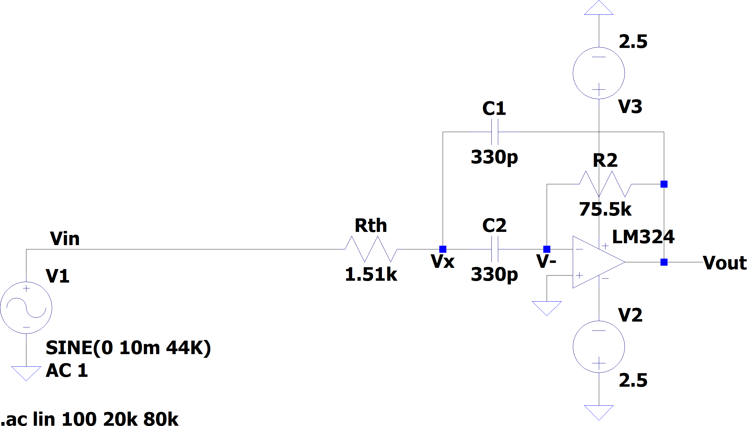
Some time ago, for this project, I designed an active bandpass filter. To simplify its design, I used a 10 MHz GBW op-amp. However a lower GBW op-amp is a much better test for the equation taking into account the GBW.
A common and low cost op-amp is the LM324, with a GBW of 1.2 MHz. When making PCBa with JLCPCB, not only the LM324 is very cheap, but there is no component fee.
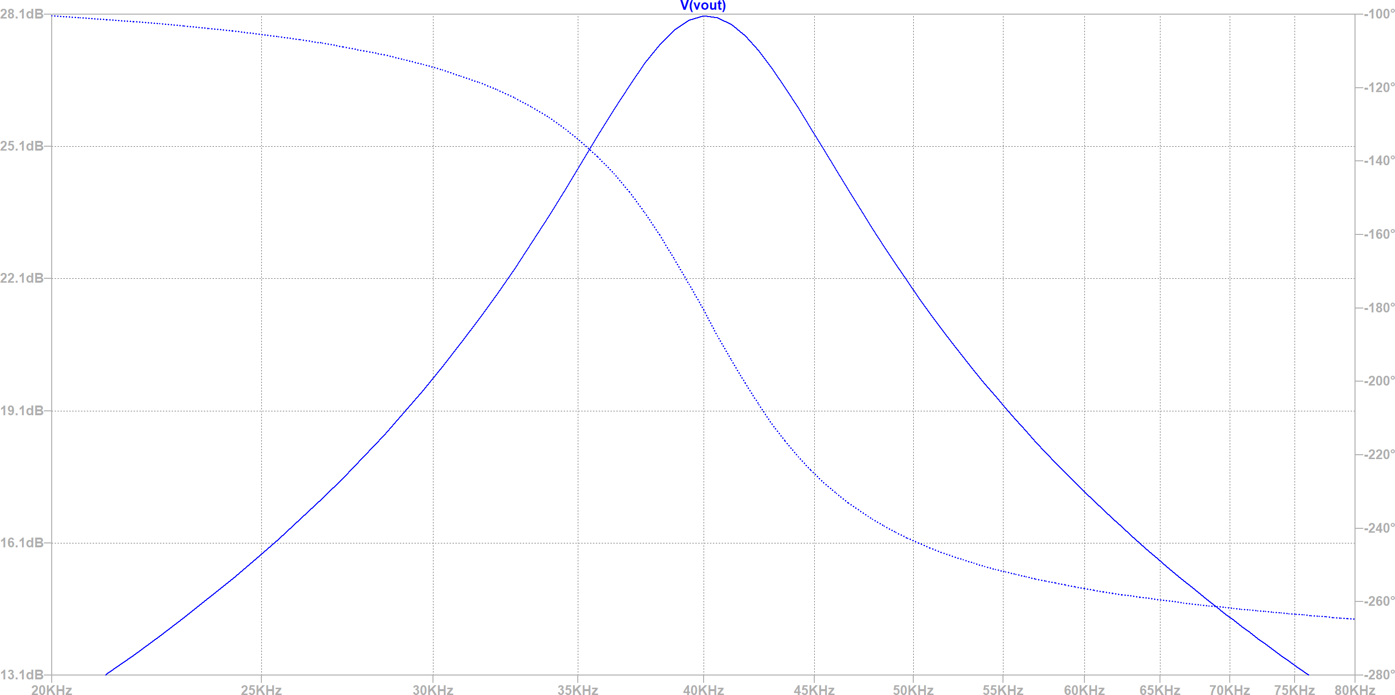
The following example filter with a 1.2 MHz GBW LM324 is designed for a 40 kHz center frequency and a 10 kHz bandwidth. Schematic and simulation results are shown below:
The Excel spreadsheet can be downloaded here and the other files in github
Conclusion
The conclusion will be written in a future release. In the meantime, please find instead a beautiful cat.
Appendix: details of the mathematics
The detailed demonstration of theses equations is a bit long, so it is put in this separate page.
 RF cat corner


 Cats fighting, from Wikipedia.