RFID coils should not be grounded.
22 Mar 2022Putting a solid ground plane in a PCB is a good practice. This allows to have good interconnexions between the different grounds of the components, to have a proximity shielding of the lines, and to reduce the cross coupling between the lines. All these effects have one root cause: a ground plane reacts to an electric or magnetic field by generating induced currents which tend to reduce this incoming field.
Due to these currents, the ground plane tends to mirror the lines: when you have on one side a line in which circulates a current, all things behave like there was a symmetrical copy with an opposite current on the other side.
Of course, for various reasons, this effect is not perfect. However, still very efficient.
However, for the very same reasons, it’s not a good idea to put a ground plane straght below an NFC coil. An NFC coil is precisely designed to make coupling to circuits in proximity, and a ground plane reduces this coupling. Nobody would make this on purpose, but this error is easy during the rounting stage.
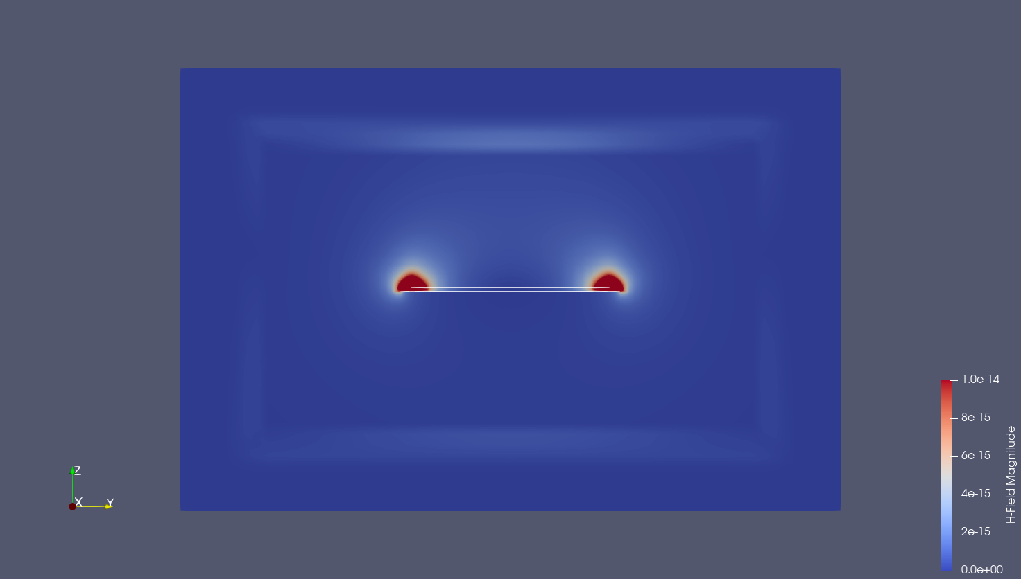
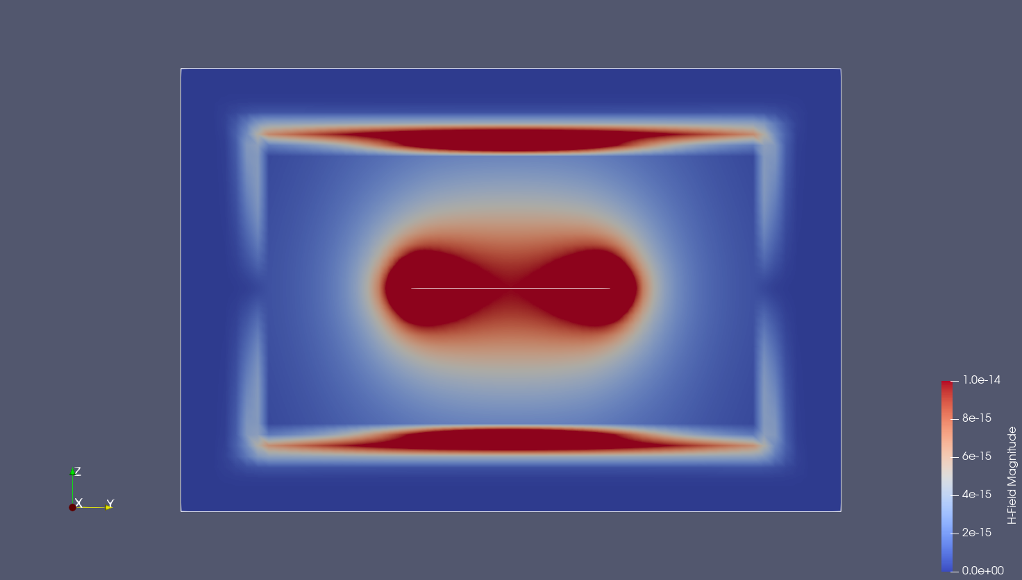
The following pictures produced with OpenEMS shows clearly this effect:
|
|
|
|
|
|
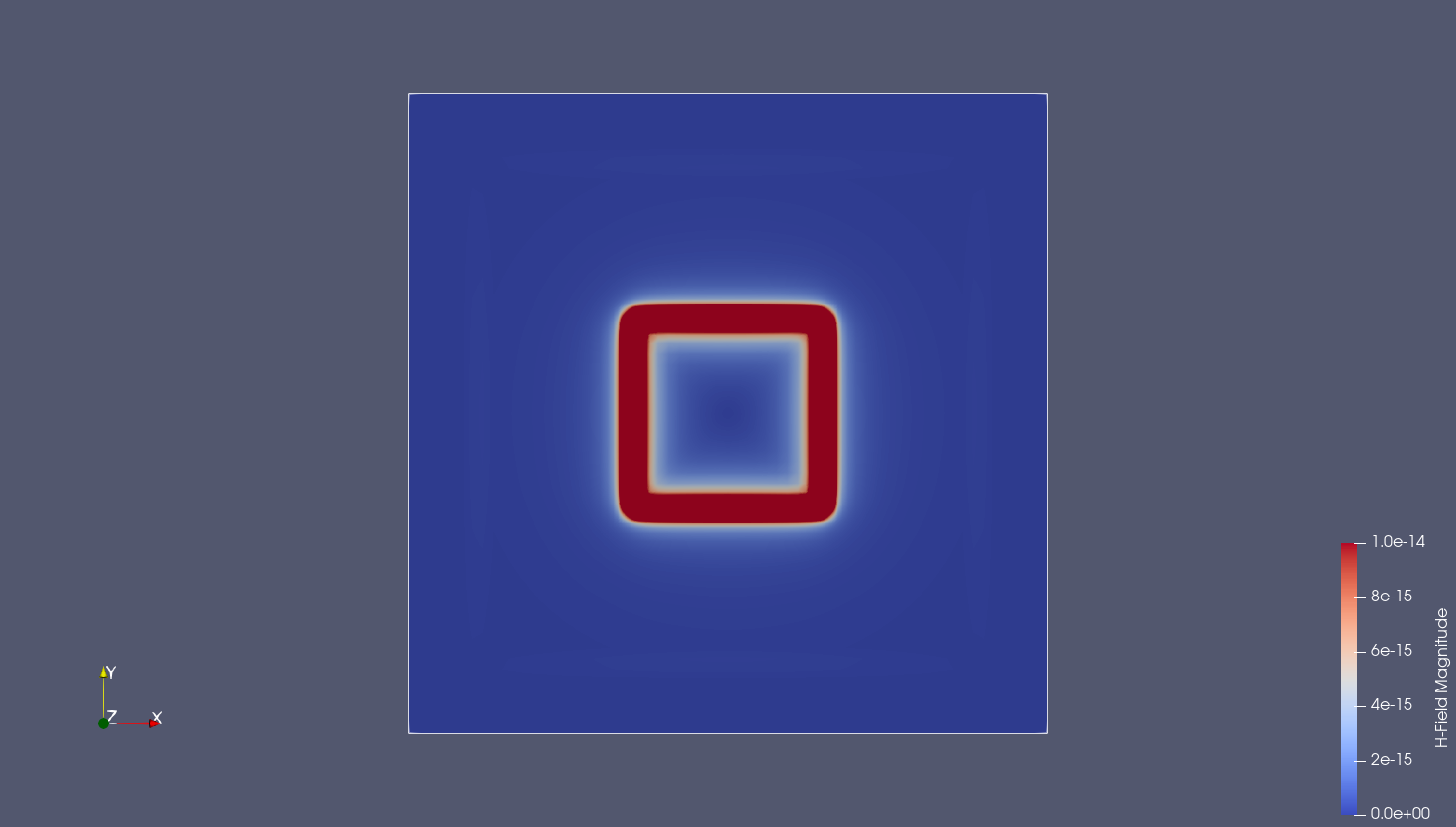
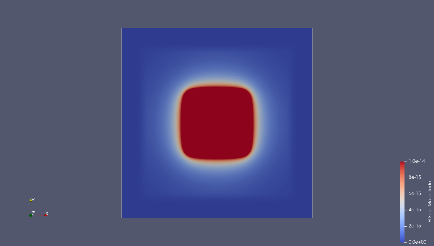
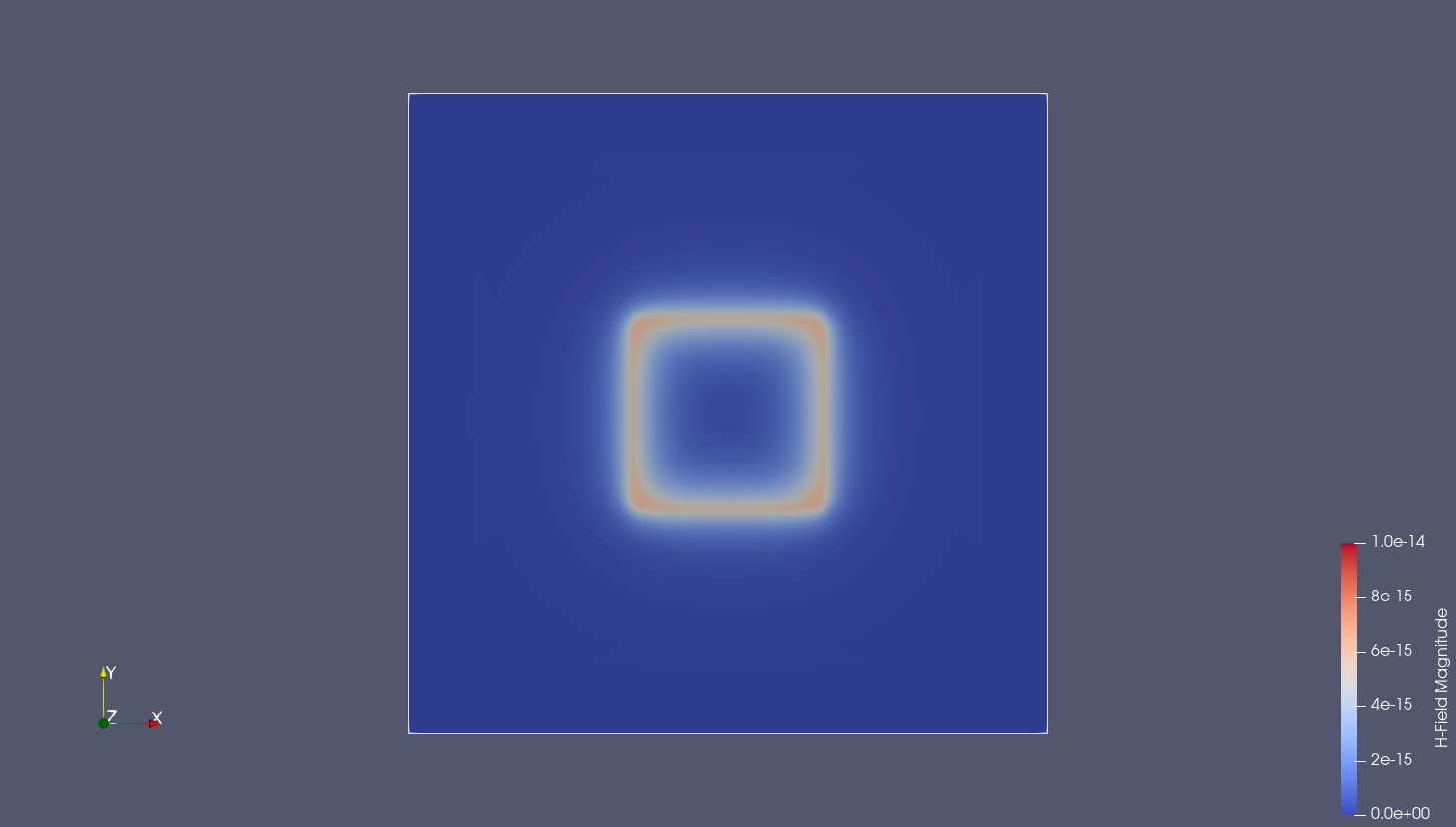
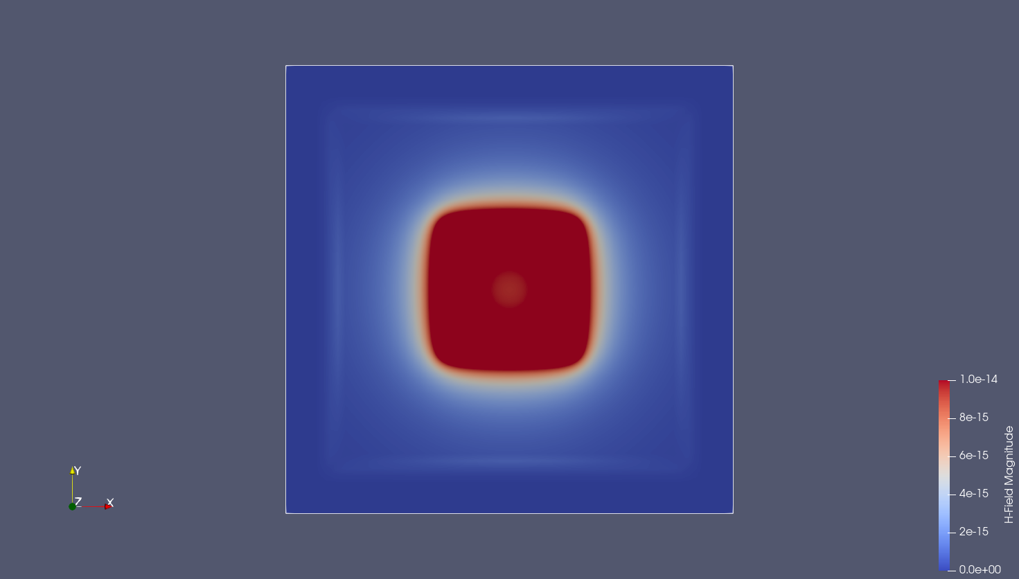
Magnetic field is shown in all figures. Left side are with a solid ground plane, right side is without. Line 1 is between the coil and the bottom of the PCB. Line 2 is at 10 mm height. Last line is a perpendicular cut.
The strange box around the loop which can be seen in the different pictures is a simulation artefact explained in footnote1.
First line shows that even inside (!) the PCB, the grounded coil tends to guide the field just below it. Nothing would happen in the center. This behavior is the expected behavior of a transmission line: take a wave on one side, transport it towards the other sides, and radiate as little as possible. On the contraty, the coil behaves like a coil and the center has an high magnetic field.
Second line shows at a distance2 of 10 mm, proximity shielding reduces the generated fields in the ground plane case (left). On the contrary, without it, the magnetic field is high and would easily couple an NFC tag.
Third line shows an X-cut, which allows to see the variation of the magnetic field in function of the height. Left pictures shows that it decreases quickly with height where a ground plane is used, while this decrease is lower when no ground plane is used.
The distance where the magnetic field is highly attenuated is proportionnal to the distance between the coil and the ground plane in the first case, while it is proportional to the coil size when no ground plane is used. In this case, it is possible to increase this distance simply by increasing the coil size.
In conclusion, by the proximity shielding effect, a ground plane defeats the whole purpose of a NFC coil, which is to couple nearby circuits. To avoid this problem, remove the ground plane below the coil, and let enough distance between the NFC coil and the ground plane of the circuits using it.
-
This artefact behaves like a metallic box with microwave absorber covering its walls and preventing reflexions. This technique allows to simulate structures like they would be in an infinite space while using a finite amount of computer memory. ↩
-
More precisely, the distance to the ground plane, the PCB having some thickness. ↩
 RF cat corner