Many thanks to my management at Eutelsat who kindly allowed me to republish this document I wrote for internal use here. Many thanks to my fellow colleagues for their help in this document.
Introduction
Power amplifiers have a limit on the maximum power they can amplity while staying linear, that is, keeping distorsion low enough.
For sinusoidal signals, it is straightforward to keep the power of the signal below the maximum linear power. However, for multi-carrier signals, the signal has peaks much higher than its average power, and keeping these paks below the maximum linear power requires to have a maximum power much higher than the average power, which is costly and inefficient in power.
Since these peaks are rare, it is possible to accept that some peaks go beyond the maximum linear power, provided that the resulting distorsion is acceptable. This allow to reduce the difference between the average power and the maximum power of the amplifier.
The needed difference between the average power and the maximum power, called backoff, is not straightforward to calculate for multi-carrier signals. This article proposes an investigation of this topic and guidelines to estimate the needed backoff.
The multi-carrier signal occurs either due to multi-carrier modulation schemes or when an amplifier serves multiple users.
Existing rules of thumb do not provide a precise method to make a compromise between an high backoff, which wastes power, and a low backoff, which may not provide enough linearity. The peak to average power ratio (PAPR) is insufficient since it does not indicate how often peak levels are reached.
Modelling
An ideal amplifier has a linear transfer function in an infinite range.
Real amplifiers have a limited linear range and their transfer function is closer to the saturated cubic model of following curve.
This saturated cubic function is hard to model so the cubic model, valid for signals lower than saturation of the amplifier, is used instead. This is the domain of most often used in telecommunications.
This cubic transfer function can be expressed by the following equation:
y = x - \alpha \cdot \left|x\right|^2 \cdot x
Signals are modelled as a complex amplitude at amplifiers centre frequency.
This approach is based on the works of Roblin and Versprecht.
The following assumptions are made:
Nonlinear effects are modelled as an amplitude transfer function (without phase effects, without memory effects).
Even-order terms are ignored since they produce out-of-band distortion.
Higher-order odd terms are considered negligible compared to third-order terms.
Conjugate terms correspond to reverse spectrum output signals, which are eliminated through filtering.
Gain is normalized to unity because all variables of interest are normalized to output (OIP3, Psat, …).
Units and impedances are ignored: \text{power}=\left|x\right|^2. No \sqrt{2} is present in the power formula because complex sinusoids are considered instead of real sinusoids.
Parameters in function of OIP3
An input signal x consisting of two equal-amplitude complex sinusoids at angular frequencies ω_1 and ω_2 is considered:
x = A \cdot \left( e^{j \cdot \omega_1 \cdot t} + e^{j \cdot \omega_2 \cdot t} \right)
where A is the amplitude of each sinusoid.
To compute the tones produced by the transfer function:
A multi-carrier signal, at both input and output, which may or may not be at the same frequency, is modelled by its complex amplitude centred on the device’s centre frequency:
\begin{gather*}
x_\text{mod}(t) = \text{Re}\left[x(t) \cdot e^{j \cdot \omega_c \cdot t}\right] \\
x(t) = x_1(t) + ... + x_n(t) \\
x(t) = a_1(t) \cdot e^{j \cdot \omega_1 \cdot t} + ... + a_n(t) \cdot e^{j \cdot \omega_n \cdot t} \\
\end{gather*}
The complex amplitudes x_i(t) contains not only the base complex amplitudes of the signals a_i(t) but also the frequency shift \omega_i-\omega_c of each signal relative to the device’s centre frequency. a_i(t) can be modelled as a complex random variable without rotational symmetry. However, due to the frequency shift, x_i(t) can be modelled as a complex random variable with rotational symmetry.
The sum of the complex amplitudes x(t)=x_1 (t)+...+x_n(t) can be approximated by a zero-mean Gaussian probability distribution with a variance corresponding to its power. The following curve1, for a rolling dice, shows that starting from 3 rolls, the curve is close enough to gaussian.
To simplify calculations, the input/output power is normalized to 1, so:
The total power of x is normalized to 1 so the power of its real and imaginary components are both \frac{1}{2}. In mathematical terms, x follows a standard complex normal distribution, so \text{Re}[x] and \text{Im}[x] both follow2 a normal distribution of variance \frac{1}{2}. Consequently, 2 \cdot s follows a Chi-squared probability distribution3 with two degrees of freedom, itself equal to an exponential distribution of parameter \frac{1}{2}, whose moments can be calculated as such4:
The quantity \text{OIP3}_\text{dBm} - P_\text{sat,dBm} will be called in the following \text{LF} for linearity factor because it it higher when the amplifier is more linear. Estimations of this quantity will be given in the following sections.
The quantity P_\text{sat,dBm} - P_\text{out,dBm} is called the \text{OBO} for output backoff and can be expressed as:
Values of the linearity factor LF for different technologies
The previous equations for the calculation need \text{LF} =\text{OIP3}_\text{dBm} - P_\text{sat,dBm}. To have estimates of its value, a review of several typical amplifiers was performed.
The value of LF depends on the technology but is surprisingly constant inside a given technology. It is this possible to calculate recommended backoff values for each technology.
The discrete Hilbert transform seems rather mysterious. However, the principle as well as his mathematics are not so complicated: the Hilbert transform is mainly a way to add a 90° phase shift to a signal and its equation can be explained from simple mathematical principles and an Excel spreadshet.
Pulse
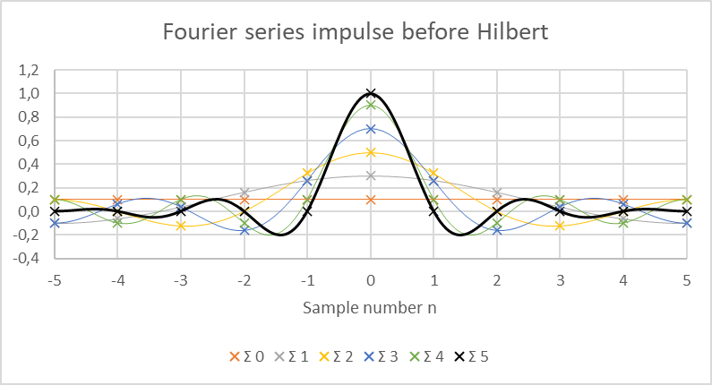
The first step is to start with a discrete unit pulse sampled using 11 points: the center point at 1 and the others at 0. For parity reasons, only 6 sinus are needed in the discrete Fourier transform.
Note that in the equation, not only the discrete points are calculated, but also the points in between to have curve easier to visualise. This smoothing is similar to a reconstruction filter.
Transformed pulse
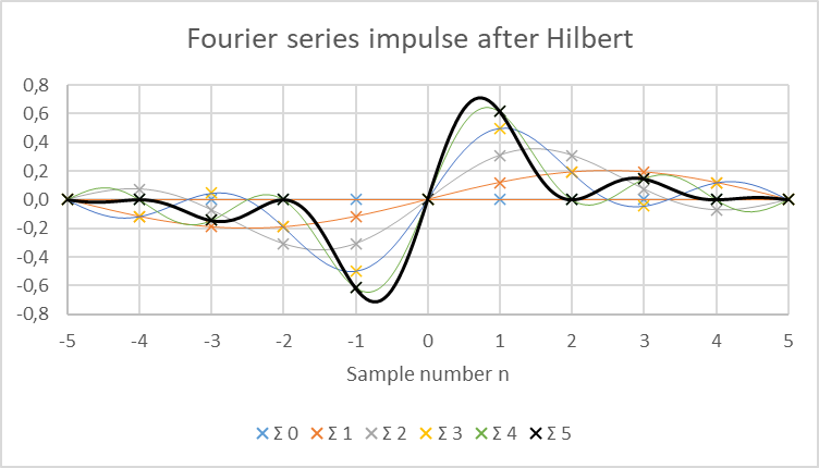
The next step is to apply a 90° phase shift to all the sinusoids of the previous sum.
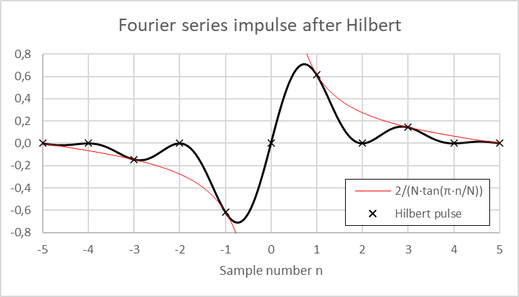
The resulting sum gives the Hilbert transform of the starting pulse. It is compared to the mathematical equation of the discrete Hilbert transform of a pulse for a finite number of samples in the following plot. Note that the red line gives the value of the transform only for the odd points, the others being at 0.
This demonstration was performed using a finite number of samples, rather small. In real cases, the number of samples is likely to be infinite, either as an approximation or a big number of samples or as a continuous flow like in software defined radio (SDR). The question of the practical implementation of these cases is left aside. For an infinite number of samples, the limit can be calculated as follows:
2025-12-21: Replace statically generated plots by dynamically generated and interactive plots using plotly.js. Note the javascript code is also for you: if you need to calculate such structures, feel free to have a look on it.
2025-11-09: Fix roots calculation and change of variables.
2025-10-26: Fix some errors in formulas, add some details about calculations.
2023-06-25: First version.
This blog page is an English translation and adaptation of a part of my PhD thesis. Numbers in brackets refers to the original bibliography, they will be replaced in a future revision.
Impedance matching is performed by LC ladder networks. This method allows to synthesize low impedances (around 5 Ω) on the same PCB than the standard 50 Ω output (no need for a second PCB with high permittivity). Moreover, this method is more compact than quarter-wave transformer.
Exact value calculation was performed by numerical optimization. Manual calculation would be too difficule because the output impedance of the transistor is not a pure resistance1. However, numerical optimization needs to know the number of components of the ladder, because the ADS optimizer is not able to add components when needed, but is only able to determine their value. Moreover, an initial estimate of the values of the components of the LC ladder is useful for the optimizer to converge quicker towards the solution. Calculation method is the one of 2, adapted for the needs of the PhD thesis.
Inductors and capacitors are assumed ideal and lossless, as well as the microstrip junctions. The effets of the polarization networks of the transistors are also ignored. Such effects are absolutely not negligeable, but will be easily corrected by the numerical optimizer in the final phase of the design.
A simple empirical method is commonly used 3, but it doesn’t allows a priori calculation of the order and of the mismatch of the matching network.
In 4 and 5, tables of 2 are used to calculate a low-pass matching network of Chebychev type. Unfortunately these tables does not provide values for very broadband impedance matching network (1:6 ratio for the amplifier module of the PhD thesis).
For these reasons this page describes in detail the calculation of such impedance matching networks. The calculation method is the one of 2, adapted for the needs of the PhD thesis.
As usual, f is the usual frequency in s^-1 and \omega the angular pulsation in rad \cdot s^-1. Calculations will use mainly \omega.
In a first time, the matching network is calculated for the center frequency \omega_0=1 and source 2 to test the good operation of the Python program which was written during the PhD thesis.
The reflexion coefficient of a LC ladder (output) matching network of type Chebychev, seen from the source, is6:
with7\omega_0=sqrt((\omega_a^2+\omega_b^2)/2), \Delta\omega^2=(\omega_b^2-\omega_a^2)/2, \omega_a the beginning of the passband, and \omega_b the end of the passband.
Next figure shows the reflection coefficient seen from the source of an example of an (output) LC matching network going from 5 Ω towards 50 Ω from 1 to 2,5 GHz. These values are approximately those of the first wideband amplifier of the PhD thesis.
Fig. 1. Example of squared reflection coefficient seen from the source of an LC matching network. See text for parameters.
In previous expression, \epsilon is chosen such as:
|\Gamma(f=0)|^2=((Z_2-Z_1)/(Z_2+Z_1))^2
This last condition is needed because LC ladders have no effect in DC. So, the transfert function is entirely determined by the order and the &&Z_2/Z_1&& ratio.
In the passband, maximum reflection coefficient and maximum insertion losses are respectively:
The first step of the calculation is to determine the first n such as |\Gamma_max|^2 is less than the requirements. This calcul is done numerically, by testing all the integers n from 1 until this requirement is met.
This n is half the number of elements of the final network 2.
Next, variable change p = j · ω is performed. This variable change enables to simplify greatly the calculations to come. Then, the square of the magnitude of the reflection coefficient is factored as such:
with a and b two polynomials whose roots have negative real parts8.
With this factorization, reflection coefficient (and not only his squared norm) can be calculted as such:
\Gamma(p) = (a(p)) / (b(p))
At the beginning of our work on the subject, factorization was performed numerically. This method was thereafter discarded due to numerical instability problems for high orders. This is why a semi-analytic method was taken, inspired by [47, 84]. Roots of the numerator and of the denominator are calculated analytically. Next, factorized polynomianls are calculated by taken only roots with negative real parts.
The calculation, more long than complex, won’t be detailed. The roots of the numerator and of the denominator are given by the following formulas9:
In the implementation of this method, the negative real part roots are sorted numerically.
Fig. 2. Roots of the numerator in the example. The roots of the numerator are double and purely imaginary.Fig. 3. Roots of the denominator in the example. The roots of interest are marked in blue, while the ones in red are ignored.
A polynomial is defined by the set of its roots, but up to a multiplicative factor. The next step is to determine this multiplicative factor. Details of the calculation won’t be given here, but only the result:
with &&a_1&& and &&b_1&& the polynomials initially determined.
Next, the input impedance, normalized10 with respect to Z1, is calculated as follows:
Z(p) = (b(p) + a(p))/(b(p) - a(p))
This impedance is then expanded into a continued fraction through successive divisions:
Z(p) = g_1 \cdot p + 1 / (g_2 \cdot p + 1/ (g_3 \cdot p + ... + 1 / (g_m \cdot p + g_(m+1))))
This expression immediately leads to an LC network. The odd gm values are the normalized values of the inductances, while the even gm values are the normalized values of the capacitances. This denormalization is performed according to the following equations9:
{: ( L = g / (2 pi f_0) \cdot Z_1 ),
( C = g / (2 pi f_0) \cdot 1 / Z_1 ) :}
The last &&g_m&& is the load resistance, which is also normalized. Its value has been known for a long time, but it can be interesting to recalculate it to verify that there is no significant error due to numerical inaccuracies.
Appendix: equations of the roots
Numerator
The roots of the numerator, without any attempt to remove duplicates, can be expressed as such:
\begin{align*}
& \epsilon^2 \cdot T_n^2(x) = 0 \\
\Leftrightarrow \enspace & T_n^2(x) = 0 \\
\Leftrightarrow \enspace & \cos \left[ n \cdot \arccos (x) \right] = 0 \\
\Leftrightarrow \enspace & n \cdot \arccos x) = \frac{\pi}{2} + k \cdot \pi, \enspace k \in \mathbb{Z} \\
\Leftrightarrow \enspace & x = \cos \left[ \frac{\frac{\pi}{2} + k \cdot \pi}{n} \right], \enspace k \in \mathbb{Z} \\
\Leftrightarrow \enspace & x = \cos \left[ \frac{\pi}{2 \cdot n} \cdot \left( 1 + 2 \cdot k \right) \right], \enspace k \in \mathbb{Z} \\
\end{align*}
Due to the periodicity and invariance by sign change of the cosinus, different values of k can lead to the same root. Two different values of k lead to the same root on the following condition:
And for the same reason as for the numerator, k can be restricted to the interval [0; 2n-1].
Next, omega and p can be calculated in a similar way than for the numerator.
It is not even a pure impedance. See the blog pages to come! ↩
G.L. MATTHAEI. « Tables of Chebyshev impedance-transforming networks of low-pass filter form». In : Proceedings of the IEEE 52.8 (august 1964), p. 939-963. ISSN : 0018-9219. DOI : 10 . 1109 / PROC . 1964 . 3185. ↩↩2↩3↩4↩5
Chen CHI, Chen JUN et Wang LEI. «L-band high efficiency GaN HEMT power amplifier for space application ». In : Radar Conference 2013, IET International. Avr. 2013, p. 1-4. DOI : 10.1049/cp.2013.0455. ↩
D.A. SUKHANOV et A.A. KISHCHINSKIY. « High efficiency L-, S-, C- band GaN power pulse amplifiers ». In: Microwave and Telecommunication Technology (CriMiCo), 2013 23rd International Crimean Conference. Sept. 2013, p. 94-95. ↩
Kenle CHEN et D. PEROULIS. « Design of Highly Efficient Broadband Class-E Power Amplifier Using Synthesized Low-Pass Matching Networks ». In: Microwave Theory and Techniques, IEEE Transactions on 59.12 (déc. 2011), p. 3162-3173. ISSN : 0018-9480. DOI : 10.1109/TMTT.2011.2169080. ↩
There was a typo in these formulas in a previous version of this article. Sorry. ↩
Such polynomials are called Hurwitz polynomials. The reasons why a and b must satisfy this condition go beyond the scope of this thesis. The reader is encouraged to refer to a book on network synthesis [12, 56, 73]. ↩
There is a typo in these formulas in the PhD thesis pdf. Sorry. ↩↩2
This point has been forgotten to be mentioned in the PhD thesis pdf. Sorry. ↩
A few years ago, I had to terminate a differential amplifier in single-ended input. Analog Devices AN-09901 gives equations for that. Unfortunately, there are an inaccuracy in these equations. According to this page, the input impedance for balanced differential input signals is given by R_"IN, dm"=2\cdotR_G and for a single-ended input by R_"IN, cm"=R_G/(1-R_F/(2\cdot(R_G+R_F))).
However, in this use case, the last equation is uncorrect. It would have been correct if the -DIN input were connected directly to ground. However, this is not the case, and instead this input is connected to ground through a resistor of value R_S////R_T to ensure symmetry.
Schematic
The schematic is shown below. Note the strange alignment of Rsp and Rsn. Rsp is part of the source while Rsn is part of the board. Note that in an actual implementation, Rsn and Rtn are likely to be merged. Details of the LTSpice simulation will be described at the end.
Calculation philosophy: solving vs. enforcing
There are two methods to calculate the values of the components in an electrical circuit:
Determine all the equations of all the wanted parameters (gain, impedance) in function of the components values, and invert all the equation. This is the solving approach.
Enforce at as soon as possible in the calculation process the wanted parameters by setting early some components values. This is the enforcing approach.
Calculations get much easier with the enforcing approach, in a similar approach than proposed by Middlebrook and its successors, notably Vorperian and Basso.
This case is a great illustration of this principle. I first tried the first approach, without success, thereafter the second approach, and got manageable equations.
Calculations details
Calculation of RG
It is assumed that RF is fixed. For current feedback amplifiers, common for high speed, RF contributes to the amplifier gain and have a value recommended by the datasheet which should be respected in most cases. For voltage feedback amplifiers having some speed, RF have to be low enough to avoid issues with the various parasitic capacitances which also leads to a recommended value.
Normalisation
After a long time working with these equations, I realized it was easier to use normalized values of the resistors, and the easiest value for normalization is the feedback resistor RF, as such:
In which the values of &&V_X^+&& and &&V_X^-&& can be substituted:
\begin{split}
V_S \cdot K \cdot \frac{1}{R_G^{'}}-G\cdot V_S &= V_S \cdot K \cdot \frac{1}{\frac{2\cdot\left(1+R_G^{'}\right)}{G\cdot{R_S^{'}}}-1} \cdot \frac{1}{R_G^{'}} \\
K - G \cdot R_G^{'} &= K \cdot \frac{1}{\frac{2\cdot\left(1+R_G^{'}\right)}{G\cdot{R_S^{'}}}-1}
\end{split}
\left[ K - G \cdot R_G^{'} \right] \cdot \left[ \frac{2\cdot\left(1+R_G^{'}\right)}{G\cdot{R_S^{'}}}-1 \right] = K
Which can be put in a second order equation in the following way (note the early optimizations of the equations):
This quadratic equation can be solved in the usual way3:
A = 1
B = 1 - \frac{G \cdot R_S^{'} }{2} - \frac{K}{G}
C = K \cdot \left( -\frac{1}{G} + R_S^{'} \right)
\Delta = B^2 - 4 \cdot A \cdot C = \left[ 1 - \frac{G \cdot R_S^{'} }{2} - \frac{K}{G} \right]^2 + 4 \cdot K \cdot \left( \frac{1}{G} - R_S^{'} \right)
Usually, we say some things about the sign of &&\Delta&& and the existence of the roots. This will be left for a further release of this page. For now, just find the equations to put in Excel:
LTSpice simulation filed are provided here: diff-amp-SE-plot.asc and diff-amp-SE-plot.plt. Gain was set to 2 to allow easier check of proper operation by superimposing the curves.
Excel file
The Excel calculation file, self explanatory, can be downloaded here: diff-amp-SE-Excel.xlsx.
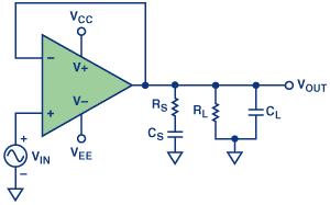
Operational amplifiers are often, and for good reason, the go-to building block of many analog functions. They are often used with capacitive loads, for two main reasons. One, when operational amplifiers are used to produce DC voltage supplies, in which cases the capacitive load is used to ensure DC voltage stays constant. Second, when operational amplifiers are used to drive some capacitive load, typically the gate of the transistor of an RF power amplifier, including the capacitors of the biasing network.
However, a common trap with such circuits is that operational amplifiers tend to be unstable when they are capacitively loaded, even for relatively low values.
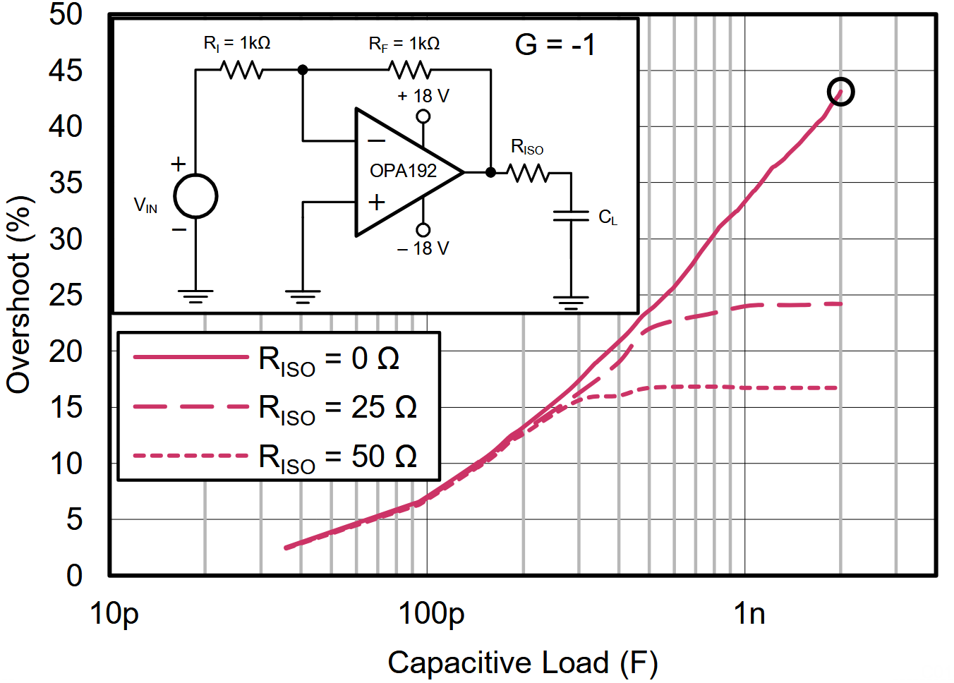
Beware of the “high capacitive load drive capability” op-amps
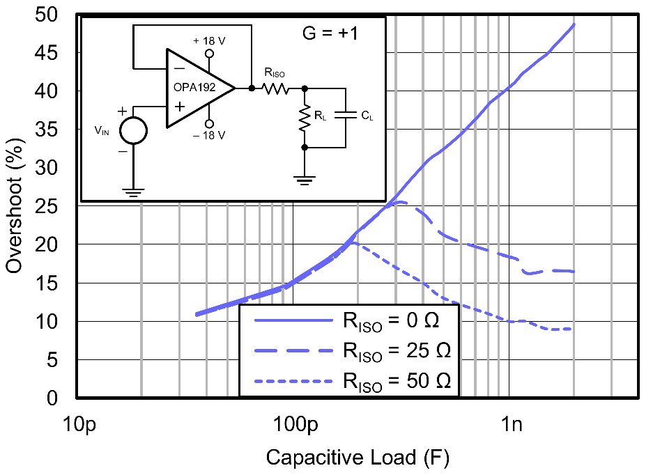
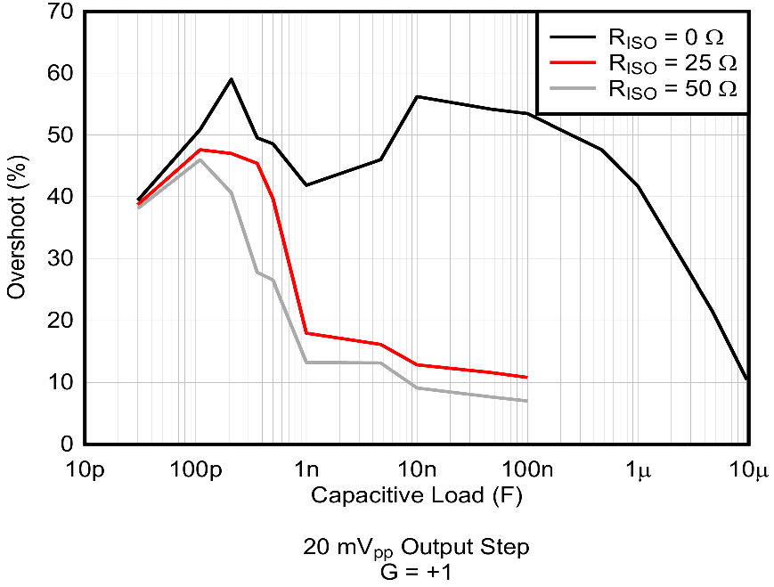
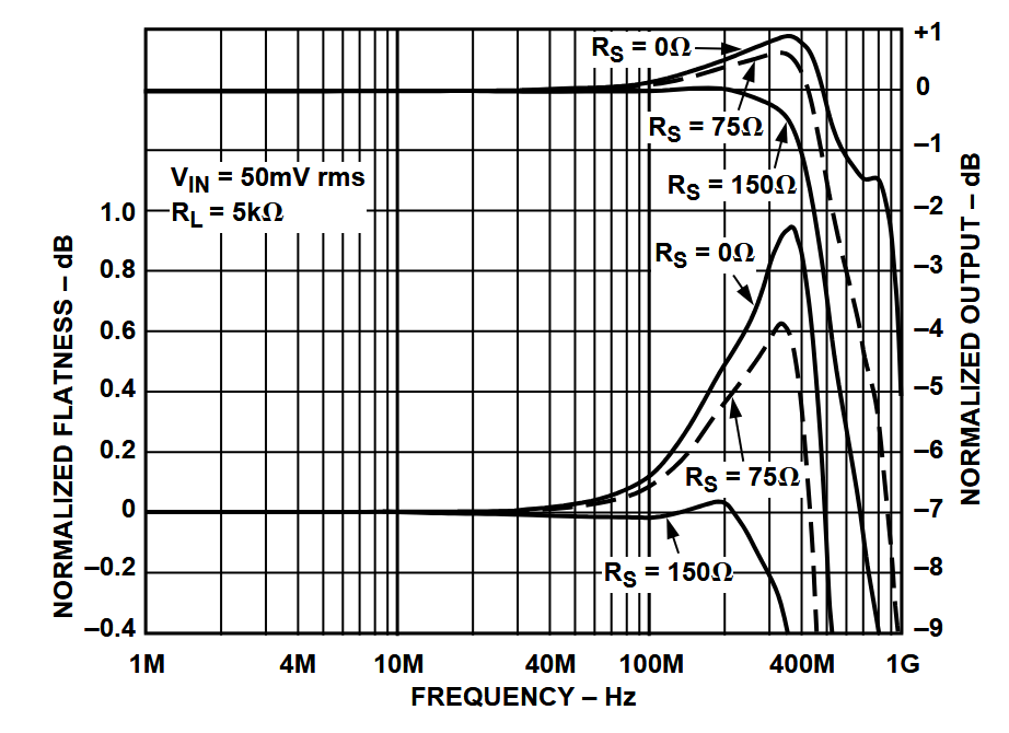
Some op-amps models like the OPA1921 advertise an “high capacitive load drive capability”, but the stated value is only 1 nF. Even if this is only a typical value, its conditions are rather fair: only 40% overshoot. The main problem is that it is only 1 nF.
The same graphs suggest that a 25 Ω improves greatly the overshoot, with a maximum value of 25 %, and allows to use an arbitrarily high capacitive load.
And once the isolation resistor is added, it lacks only two components to make something perfect. Why not read the following and add them ?
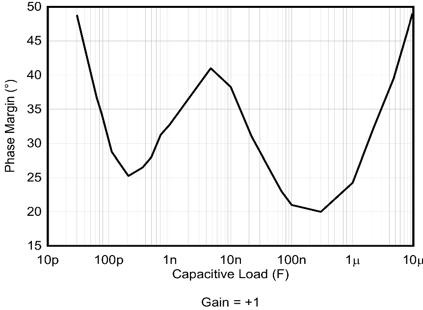
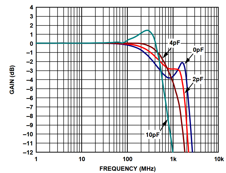
In the discussion, the OPA9942 was suggested. Indeed, it is advertised as having an “unlimited capacitive load drive capability” with a “phase margin of 50° when driving a load of 10 μF and 1 MΩ”. It is indeed the case. However, on some part of the phase margin plots, the phase margin is as low as 20°, and, again, is works much better with an isolation resistor. It should be noted, however, that the OP994 with a 50 Ω isolation resistor has a 45 % worst case overshoot while the OPA192 has only a 20 % overshoot.
And once the isolation resistor is added, same comment than before.
The root cause
A feedback system must have less than 180° phase shift from its output to its - input at the unity gain frequency in order to the negative feedback to stay negative and to avoid it going positive and causing unstability. There are more complicated ways to tell this principle but the core concepts are here.
An ideal operational amplifier has already a -90° phase shift due to its integrator nature (the gain bandwidth product). Due to various unperfections, there is also a little more phae shifting. The open loop output impedance of the operational amplifier combined with the capacitive load easily makes almost -90° phase shift at unity gain if the GBW and the capacitor are high enough. All this combined, this can lead to high overshoots, an high closed-loop output impedance, or a caracterized oscillation.
Note what matter for stability is the open loop operational amplifier output impedance. The closed loop output impedance is much lower due to feedback, at least when the feedback operates properly.
Some details on the topic
The details of the topic won’t be explained here, because the most important is to be aware of the problem and of its solutions. Once the problem is known, details are easy to find on Google. Reference 3 is a great starter, even if I would suggest an other solution on the “RC filter directly at the input”, 4 gives more informations on threee useful solutions: RISO, RISO + DFB, RISO + DFB + RFx, 5 give more solutions and details, and 6 is a rather long presentation on the general subject of operational amplifier stability which beats the topic to death, 6 gives additional details and equations on the topic. This application note from Microchip7, although not complete on compensation networks, give useful equation, useful tips for ADC interfacing and give useful information on large signal effects.
The careful reader will probably notice a mistake in the “in-loop compensation circuit” of 5: Vin and GND are inverted, as well as the - and + inputs of the operational amplifiers. Despite this mistake, the remaining of the contents is highly valuable.
Important note on coaxial cables
A important case of “capacitive” loads are coaxial cables. Their distributed nature and associated characteristic impedance and propagation time makes it differ from purely capacitive loads in ways that should not ignored. Coaxial cables loaded by their characteristic impedance, most often 50 Ω, behave like like a pure resistance. Conversely, coaxial cables driven by with a source impedance equal to their characteristic impedance behave like a pure resistive source impedance.
When it is sure a coaxial cable would be loaded by its characteristic impedance, from a stability point of view, it is just a resistor. Nothing more is needed, provided the operational amplifier can feed the requested current.
When a coaxial cable is loaded by something looking like an open circuit, typically an high impedance digital input, it is best to source terminate it, by putting a resistor between the output of the operational amplifier, wired in the usual way, and the input of the coaxial cable. The coaxial cable will be merged with the source resistor, and all will behave like the source resistor loaded by the open circuit.
Such a scheme can also be used in cases where the load is most often an high impedance but not always, because the source resistor will ensure a minimum resistance seen by the operational amplifier and avoid stability problems.
In some cases, it can be useful to terminate the coaxial cable on both sides. This has the drawback to make the final voltage half the voltage at the output of the operational amplifier, but is a robust solution.
However, when the coaxial cable is loaded by some capacitor, they must together be handled like a capacitor. Nevertheless, due to the cable propagation time, some ringing can be expected if the rise and fall times are too small compared to it. This can be avoided by ensuring long enough rise and fall times or by adding some damping resistors.
Some comments of the common solutions
Input filtering
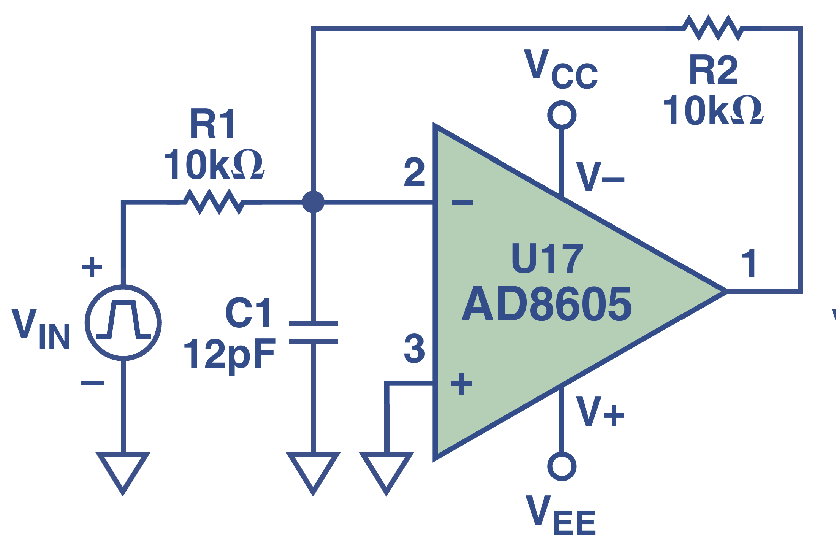
Not directly related to output driving load, this is nevertheless an interesting case to mention. Often it is derisable, particularly to reduce sensitivity to RFI and EMI, to filter the input. A capacitor straight at the op-amp inputs, like in figure below, is likely to make it unstable, for the reasons described above.
However, I would suggest an other solution than the one proposed by Analog Devices: splitting the input resistor and to put the filtering capacitor in the middle.
Output snubbing network
A perceived drawback of solutions using an isolation resistor is the voltage drop in the isolation resistor and the inability of using the full output voltage range of the operational amplifier, particularly for RRO (rail-to-rail-output) amplifiers.
Whether an isolation resistor is used or not, voltage margin between the desired voltage and the voltage rails of the operational amplifiers is useful so the retroaction loop can work properly.
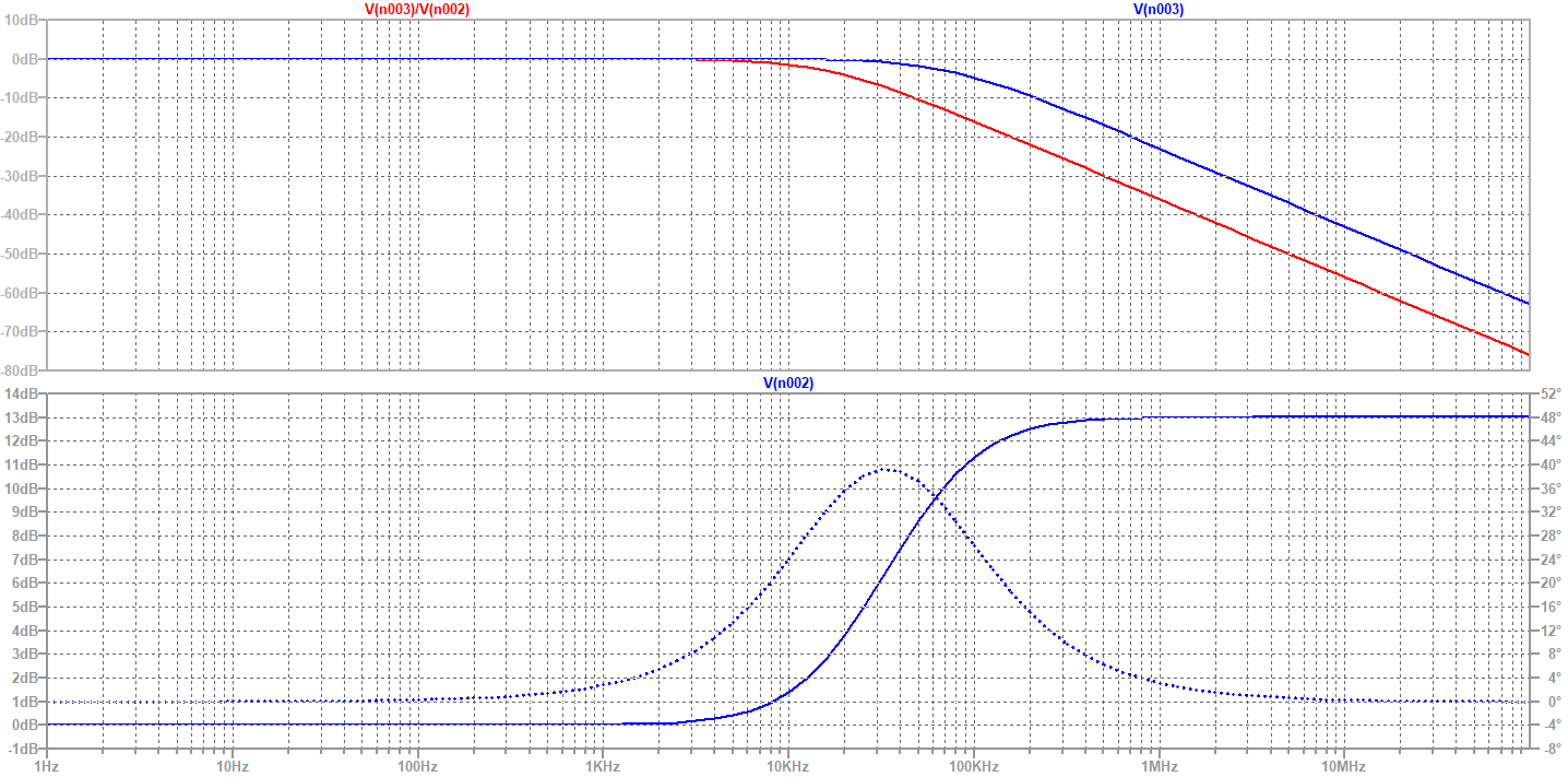
In the case this solution must be used, like in the schematic below from Analog Devices, the principle can be explained in the following simple way. RS is low enough compared to CL to make the output load looks like resistive enough to ensure a good phase margin at the unity gain frequency, while CS is high enough compared to RS to make RS+CS close enough to only RS.
This solution stabilizes the circuit, but makes the load harder to drive, making this solution ok for DC or low frequency signals, but not so much for higher frequency cases.
A tricky point of this calculation is that the needed components values depends on the unity gain frequency, but it depends itself on the values of the snubber network which tend to reduce it.
Isolation resistor
An isolation resistor ensures the opamp sees at the unity gain a convenient load, either a low enough capacitance when the capacitive load is low enough compared to the isolation resistor, or the isolation resistor when the capacitive load is high enough. This ensures stability, but at a price: the opamp produced the wanted voltage with the feedback before the resistor, and the actual voltage at the load is RC filtered.
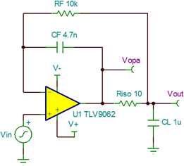
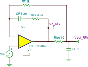
Isolation resistor + double feedback
This technique exists in two common variants shown in the 2 figures below from the excellent article4 from Texas Instruments.
The operating principle is the same in the two cases: provide an high frequency and a low frequency feedback paths. The high frequency path, right at the operational amplifier output, undelayed, provides stability, while the low frequency path, at the load, provided an exact low frequency response.
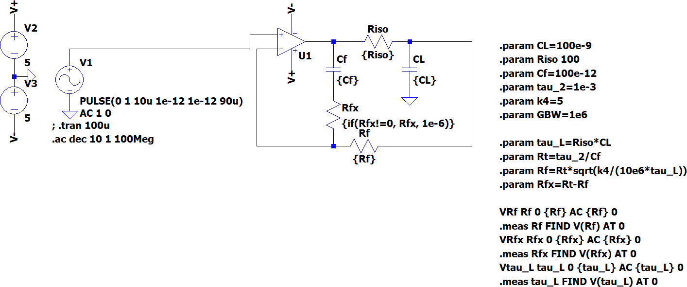
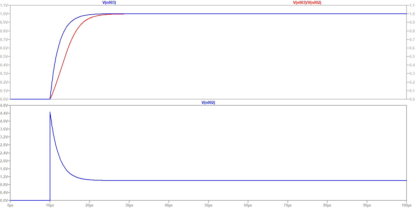
With some mathematics, it is possible to determine the optimum values which ensure both stability and performance. The detailed equations, rather long, are presented in this page: /posts/op-amp-capacitor-stability-equations.html.
Simulation results with the values calculated using the equations are shown below:
Some words on buffers
Unity gain buffer ICs can help to solve this problem, either as a standalone solution, when their offsets are tolerable, or as an addition to the opamp, kind of replacing the isolation resistors.
Since I had not yet the time to write on the topic, in waiting, please find a picture of this beautiful cat from Wikipedia:
Lately, I designed a simple biasing circuit for bipolar voltage rails (±13.5V) to bias a very precise low-noise analog circuit. To minimize offset in the analog section, it’s mandatory for the ±13.5V rails to be as closely matched as possible. The load is just a few mA, and it’s mostly a DC circuit. No fast current draws.
[...]
I did need decoupling for the biased circuit and figured 1nF would be enough. According to the OPA192 datasheet, there’s around 40 % overshoot when loaded with a [2nF, see below] cap.
[...]
The ±13.5V rails oscillated terribly.
Luckily, I had provisions to add an isolation resistor (30 ohm), and that solved the problem, though at the cost of a slight voltage drop.
I edited the message to make the total capacitive load more clear: 2 nF total, including 1 nF straight at the opamp output and 1 nF at the load.
Although some details are specific to his project, like his need of low noise, generating DC voltages to supply something is a very common need.
This circuit should not have oscillated so hard, according to the datasheet, which predicts less than 45 % overshoot for a 2 nF load.
He solved the problem using a simple isolation resistor, at the cost of a small voltage drop, and I suggested him to add a double feedback to eliminate the drop. Since it is a DC need, the simple double feedback is sufficient.
Microwaves101 gate pulser
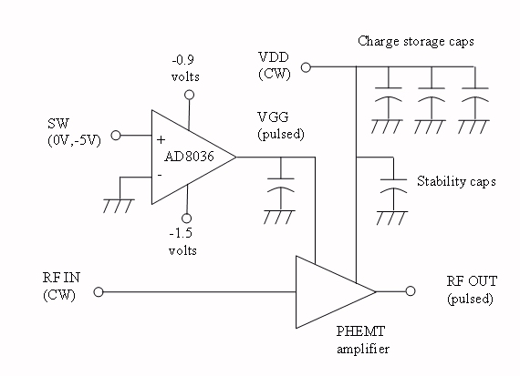
In the excellent microwaves101 website9, a page is written on the subject of pulsed RF sources. Although it advises drain pulsing (this page was written long before before GaN was mainstream), it also gives some advice about gate pulsing (bold from myself):
For a good gate pulsing circuit, we recommend the Analog Device's AD8036 "clamping amp", shown below. It lets you set up on and off gate bias voltages independently; for example, if you are using a PHEMT power amp you can set VG(on) to -0.9 volts, and VG(off) to -1.5 volts. You still need charge storage on the drain bias lines, and stability caps on gate and drain biases, as near as possible to the amp. Like all op-amps, the AD8036 can be configured as an inverting or non-inverting amplifier. Yes, we need to add some resistive feedback to the figure!
The feedback was forgotten in the figure, but not in the text.
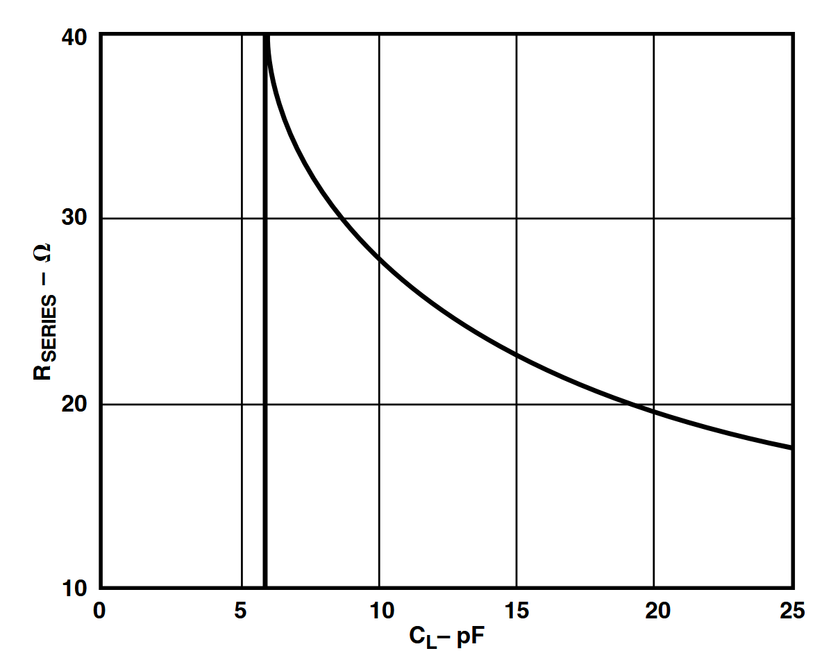
However, a point which might need to be added is the stabilisation for capacitive loads. The AD8036 datasheet does not mention performance curves when capacitively loaded, but instead a recommended isolation resistor value:
Given this curve and the typical gate bias network capacitance values, I would recommend a 20 Ω isolation resistor. The RC bandwidth is already 31.8 MHz. If not sufficient, a RISO + DFB + RFx can be used to both remove the RISO offset and to have speed up.
Microwaves101 gate pulser, alternative solution
That being said, we would propose here an alternative solution.
A problem with the AD803610 is that it is an input clamping amplifier, with clamping only available on its +VIN, making it “works only for noninverting or follower applications”. This needs a 0 to -5V input signal to have the requested VH and VL voltages. Not very convenient since most digital circuits operate on positive voltages.
Switching between two voltages levels would be conveniently done by a switch integrated circuit. Most common switches are slow, either because they are plain slow or because they include some “break before make” circuitry which take some transition times. The switches in the “buffered analog multiplexers” section of Analog Devices11 provide faster time, probably because the techniques to deal with switching transitions are easier to implement in unidirectional multiplexed buffer than in unidirectional buffer, like current steering:
The [ADV312912] multiplexer is organized as two input transconductance stages tied in parallel with a single output transimpedance stage followed by a unity-gain buffer. Internal voltage feedback sets the gain.
The following chips are interesting, with only single channel devices mentionned:
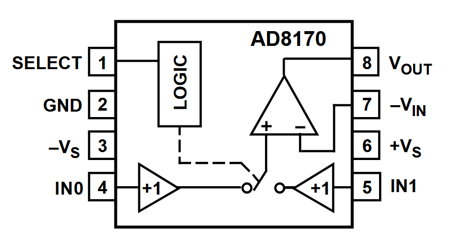
The AD8170 is a current feedback amplifier with a switchable input. These category of operational amplifiers are sensitive to the impedance seen at the feedback pin, to DFB schemes cannot be used directly with them. The datasheet recommands isolation resistor values and feedback resistance. Simple RC calculations shows that the performance is mainly determined by the RC constant of the isolation resistor and the capacitive load.
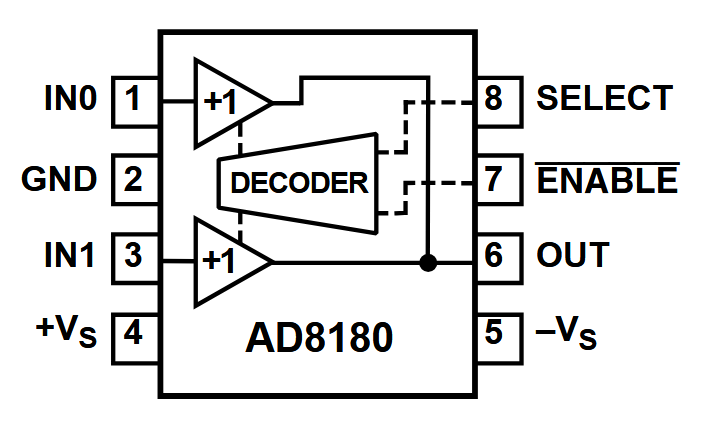
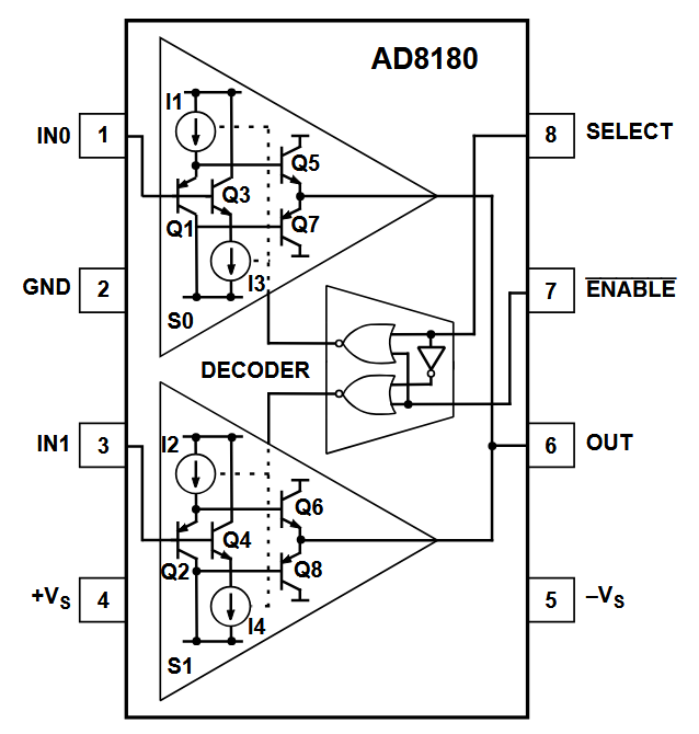
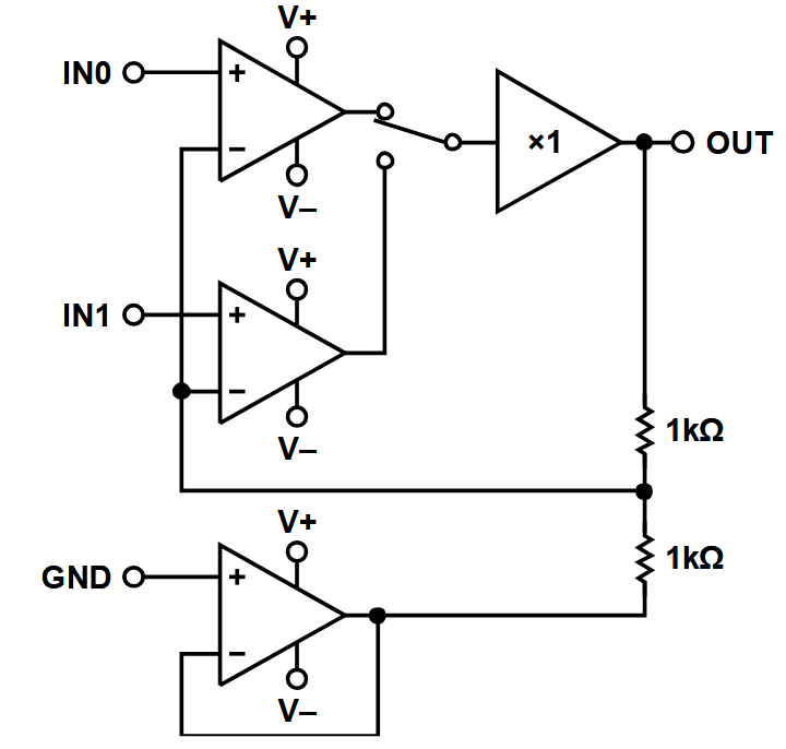
The AD8180 is an open loop buffer and can drive capacitive loads without isolation resistors. However, an input resistor is recommended. This is often the case for buffer amplifiers, and often forgotten. Performance is again determined by the open loop impedance of approximately 25 Ω.
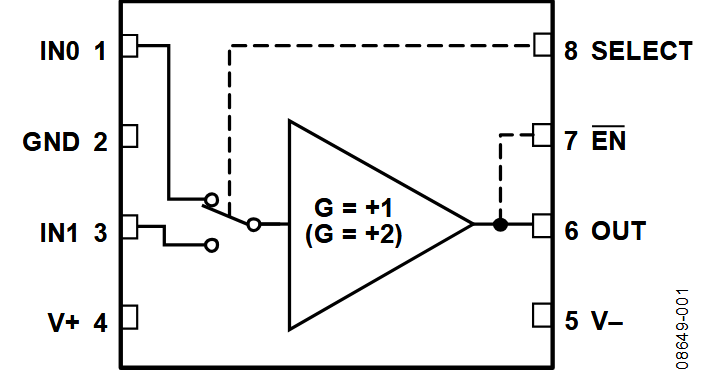
The ADV3219 is a feedback amplifier with an internal feedback. Performance curves are given for low capacitive loads without isolation resistor. For higher capacitive loads, the datasheets recommands an isolation resistor of “a few tens of ohms”, but does not give more performance details. Nevertheless it can be assumes that it will be dominated by the RC constant of the output.
AD8170
AD8180
AD8180
ADV3219
Conclusion
Capacitor unstability when capacitively loaded is a classical trap, catching even rather experienced designers, particularly RF designers who are not always proficient in low frequency analog design. Although it may seem hard, this problem is well known, well documented and has readily available efficient solutions.
Appendix
Previous version of the page included various cat pictures as placeholders for contents to be written. They are left here for posterity:
 RF cat corner


