RF cat corner
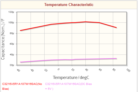
Microstrip formulas comparison.
07 Jul 2024Introduction
The designer has several tools and formulas available to calculate the characteristic impedance of microstrip lines. Some are highly precise but rather complex like the Hammerstad and Jensen formulas1,2,3, while others are rather simple but with questionable accuracy like the IPC-2141 formulas4,5,6. While approximations can be useful for the first steps of a design, their accuracy must be evaluated before use. The authors of Qucs3 made some comparison, but this comparison don’t include the common IPC formulas5,6. A comparison of the most common microstrip calculation formulas is shown here.
While Hammerstad and Jensen formulas1 stay the gold standard, other formulas can be safely used but that IPC-2141 formulas4,5,6 must be used with extreme caution.
Geometry of the problem
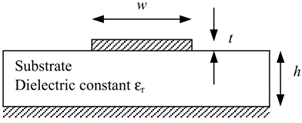
Fig. 1 – Geometry of a microstrip line4.
The geometrical parameters of the microstrip line studied are defined in Fig. 14: w is the width of the microstrip line, h the height of the substrate, t the thickness of the strip. Non-geometrical parameters are the relative permittivity of the substrate. We’ll note for the characteristic impedance of free space.
To simplify the analysis, the strip conductivity is assumed to be infinite, the substrate losses to be null, the thickness t to be null and the frequency to be null. Note that the infinite conductivity hypothesis implies the absence of low-frequency dispersion7,8. These assumptions are often used in RF and microwave design, and are of good accuracy for the impedance calculation.
Reference formula for Microstrip
Evaluating the accuracy of models needs a reference to compare to. Hammerstad and Jensen formulas are the most accurate closed-form formulas, and their accuracy is higher than manufacturing processes. They are commonly used in CAD software3,9 in which the accuracy of the models of single microstrip lines without discontinuities is recognized. However, these formulas are so complex than their practical use for a comparison can lead to type errors during implementation, which can lead to inaccuracies. 3D EM simulations can be as accurate as needed, but their setup and calculation time is time consuming when accuracy is needed. Measurements are highly expensive due to the need of accuracy in both manufacturing and characterization of board materials. So, for this setup, a well-known software is used, TXLine from AWR. This software implements probably Hammerstad and Jensen formulas and its wide use almost guarantees that the implementation is bug free.
Formulas to be compared
The formulas to be compared are the following:
TXLine
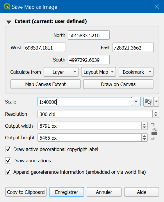
TXLine is a small software, lightweight and free to use, from AWR, which allows to calculate the characteristic impedance of transmission lines like microstrip and striplines. A screenshot is shown Fig. 2.
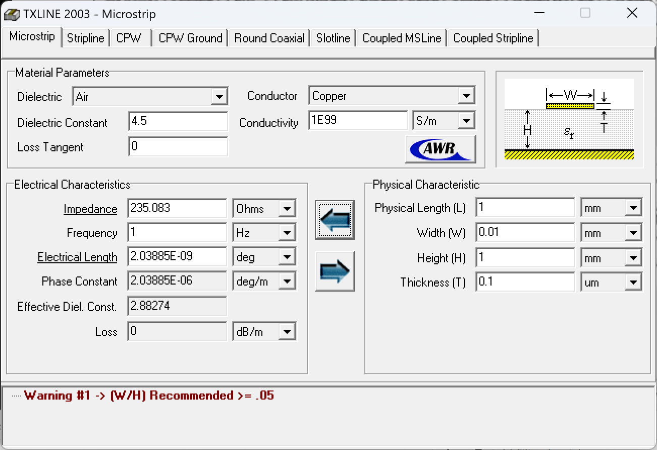
Since TXLine has no direct option to handle the infinite conductivity, the zero thickness or the zero frequency, they were approximated as follows: conductivity
Hammerstad and Jensen
According to Hammerstad and Jensen formulas1,2,3 the calculation is made in two steps. First, the effective dielectric constant is calculated:
Thereafter, the following formulas are used to calculate the characteristic impedance of the microstrip line, assuming the line is in an homogeneous medium of dielectric constant :
Note that in reference1, the formulas are not very clear about whether or should be used, but this point was double-checked in the Excel spreadsheet formulas.
These formulas are used in these calculators10,11.
Wheeler 1965
Wheeler’s formulas are sometimes encountered in technical literature3,12. They are rather accurate for most uses, as will be seen in following sections. Their main problem is the undesirable impedance step. Note that, contrary to Hammerstad and Jensen formulas, the effective dielectric constant is not used in the characteristic impedance formulas.
We have not found any calculator using these formulas.
Wheeler 1977
Wheeler 1977 formulas are seen more often than Wheeler 1965 formulas in literature4,13,14,15. They are attributed sometimes to Wadell because he made a good summary in his book13. Note that these formulas are incorrectly typed a reference4, where a
They are used in several microwave calculators17,18,19,20,21. Calculator21 has a mistake in the handling of
No explicit formula is given for
Hammerstad 1975 formulas
Often seen in websites22 or in lectures on microwave techniques23,24, Hammerstad’s 1975 formulas are the following22,25,26,27,28. They are often attributed to Bahl, who made an improvement to their strip thickness correction26,27, not investigated in this article, but the zero-thickness formulas originates from Hammerstad25.
These formulas are used in these calculators29,30,31. Note that this calculator30 also includes frequency thickness correction and dispersion.
Schneider
Not often seen, Schneider formulas3,32 are as following:
We have not found any calculator using this formula.
IPC-2141 formulas
The IPC-2141 formulas4,5,6,28 are very popular. However, despite their popularity, they should be used with extreme caution, as will be demonstrated during our comparison, because their range of validity is extremely narrow, and they have a bad asymptotic behavior.
Although they are widely quoted, their narrow range of validity is much less often quoted28:
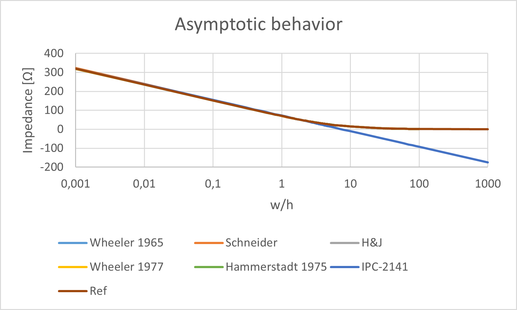
Contrary to other formulas (Hammerstad and Jensen, Wheeler 1965, Wheeler 1977, Schneider and Hammerstad 1975), IPC-2141 formulas have a totally nonsense asymptotic behavior. All other formulas were found to have an accuracy better than 1.5 % for
Fig. 1 compares the asymptotic behavior of IPC-2141 formulas with the good formulas. While IPC-2141 have a very bad asymptotic behavior for large lines, all good formulas have a good asymptotic behavior on the very wide range
Despite the problems of IPC-2141 formulas, they are used in several online calculators33,34,35,36,[^37],37,38,39. Some calculators33,34,35 give warnings when using IPC-2141 formulas outside of their validity range like shown in Fig. 3. On the contrary, some other calculators36,[^37],37,38,39 give neither a warning nor a validity range, including a calculator on a renowned website37. Worse, some calculators37,38,39 even give nonsense negative impedance when fed with proper values without any warning.
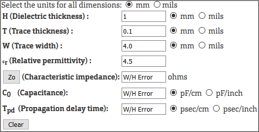
Fig. 4 – Screenshot of a microstrip line impedance calculator33 raising a warning when trying to calculate impedances outside IPC-2141 validity range.
It should be mentioned that a calculator33 not only gives the validity range of the IPC-2141 formula and warns when trying to enter parameters outside of this range, but it also gives accuracy data.
Comparison results
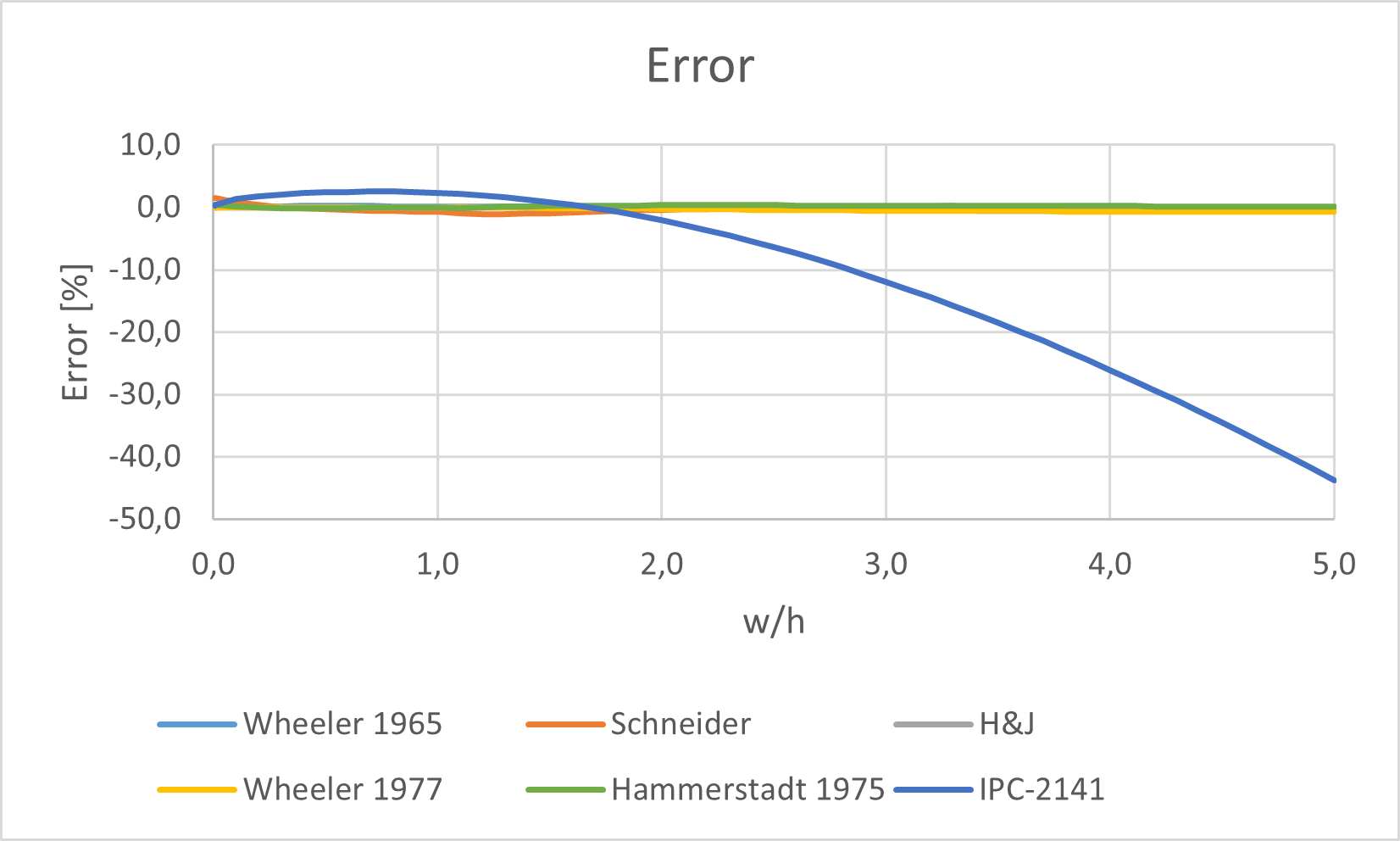
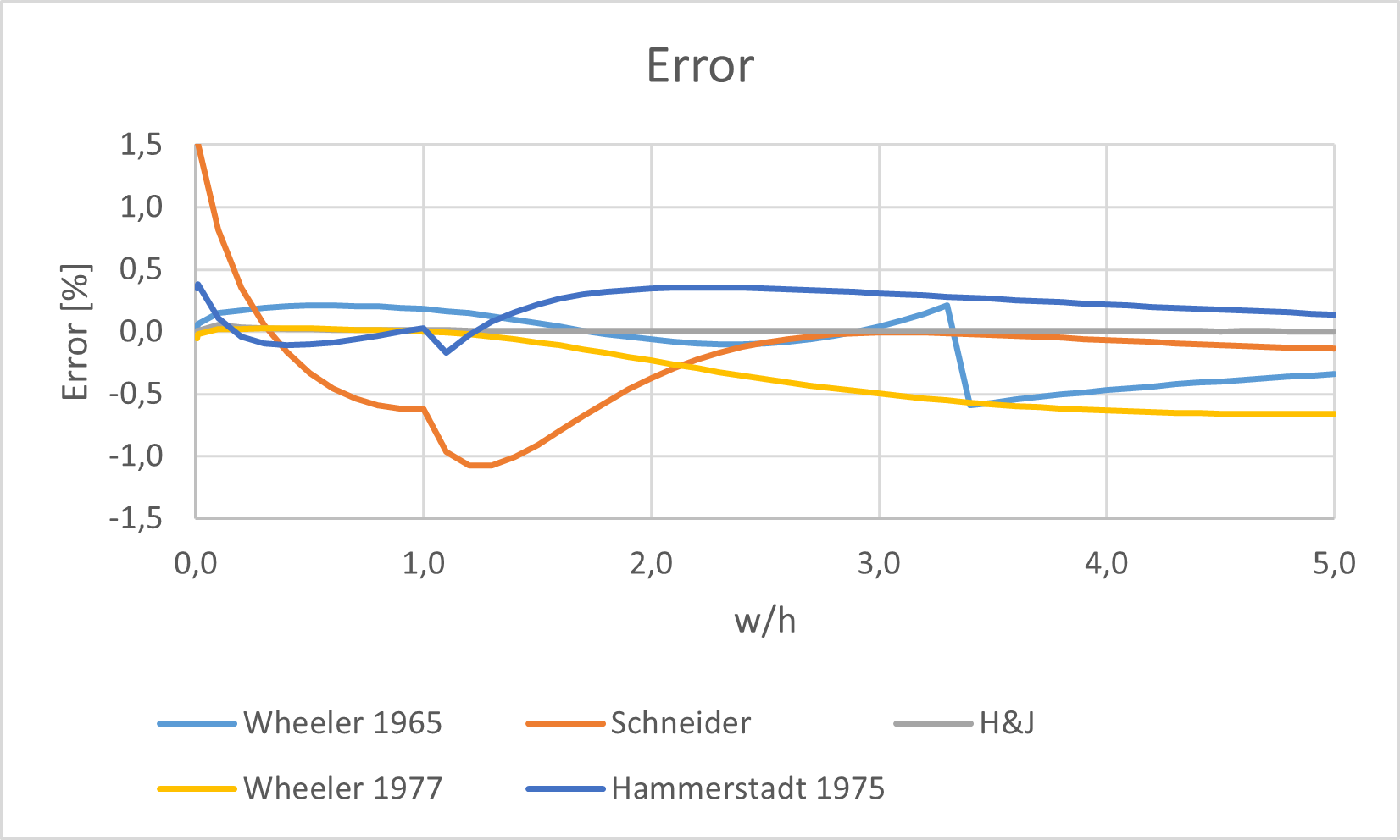
From the Fig. 5 graph, a clear outsider in inaccuracy is the IPC-2141 formula, reaching up to 44 % inaccuracy! This formula will be commented later. Fig. 6 graph, without the IPC-2141 formula on a reduced scale, shows the relative error of the remaining formulas.
The H&J formulas are probably the formulas used in TXLine software since the calculated difference between them is lesser than 0.06 % ! Note that this calculated error is always positive, because TXLine took a line thickness which is non-zero, although very thin, contrary to our calculation. Since we are comparing the H&J formulas to themselves, this benchmark does not prove that they are the most accurate. However, since they are believed to be the most accurate in all the recent literature, we’ll stick to that conclusion. They still have the inconvenient of their complexity, which can lead to potential typing mistakes.
Hammerstad 1975 formulas are at the second place for accuracy: error less than 0,38 % on tested values. However, they still have the inconvenience of their complexity, potentially leading to typing mistake, and of the different expressions for different subdomains.
Wheeler 1965 formulas are at the third place for accuracy: error less than 0.59 % on tested values. However, the calculation step makes them troublesome to use in some cases. And, for use in Excel spreadsheets, it makes mandatory to duplicate the formulas. The 0,06 % accuracy gained from Wheeler 1977 is not worth it.
Wheeler 1977 formulas, although not very known, are rather simple and rather accurate: the error is lesser than 0.66 % on tested values. The absence of impedance steps in these formulas make them interesting.
Schneider formulas are less complex than Hammerstad 1975 formulas but less accurate. Their error is less than 1.6 %. Their interest is mainly historical.
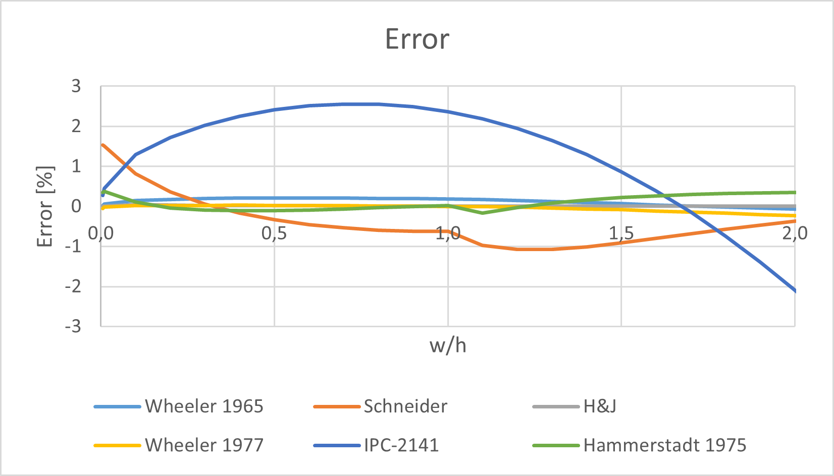
The real strange point is the accuracy of the IPC-2141 formulas. Their relative error reach 44 % on the tested values! A closer look reveals that most of the error happens when the normalized width u is higher than 2. When plotted on a narrower range, like in Fig. 7, the relative error is much lower: less than 2.1 %. This is precisely the range of values of the 50 Ω lines.
Review of calculators
The following table sums up some microstrip calculators and the formulas which they use. Only microstrip calculators for which the formula was told or could be inferred from JavaScript source code were included.
| Website | Formula | Val. warn | Comments |
|---|---|---|---|
| www.microwaves101.com10 | H&J | ||
| mcalc.sourceforge.net11 | H&J | ||
| www.eeweb.com17 | Wheeler 1977 | ||
| cepd.com18 | Wheeler 1977 | ||
| www.finetune.co.jp19 | Wheeler 1977 | ||
| leleivre.com20 | Wheeler 1977 | ||
| chemandy.com21 | Wheeler 1977 | Confusion between εr and εr,eff. | |
| www.pasternack.com29 | Hammerstad 1975 | ||
| www.emclab.cei.uec.ac.jp30 | Hammerstad 1975 | ||
| chemandy.com31 | Hammerstad 1975 | ||
| emclab.mst.edu33 | IPC-2141 | Yes | |
| referencedesigner.com34 | IPC-2121 | Yes | Formulas not told in document, but seen in JavaScript source code. |
| technick.net35 | IPC-2141 | Yes | |
| a8blog.com36 | IPC-2141 | No | No warnings, but at least does not print the calculated negative impedance. |
| www.everythingrf.com37 | IPC-2141 | No | |
| chemandy.com38 | IPC-2141 | No | |
| ncalculators.com39 | IPC-2121 | No |
Conclusion
While H&J formulas are the gold standard for calculations, several other formulas give a good trade-off between accuracy and simplicity which are sufficient for most applications. Wheeler 1977 is the clear winner of this tradeoff with 0.66 % error when
IPC-2141 formulas have severe issues and must be used with extreme caution.
-
E. Hammerstad and O. Jensen, “Accurate Models for Microstrip Computer-Aided Design,” in Microwave symposium Digest, 1980 IEEE MTT-S International, 1980. ↩ ↩2 ↩3 ↩4
-
S. J. Orfanidis, “Electromagnetic waves and antennas,” 2016. [Online]. Available (archive): https://web.archive.org/web/20240528230718/www.ece.rutgers.edu/~orfanidi/ewa/. [Accessed 14 May 2025]. ↩ ↩2
-
S. Jahn, M. Margraf, V. Habchiand and R. Jacob, “Qucs technical papers,” 2007. ↩ ↩2 ↩3 ↩4 ↩5 ↩6
-
A. J. Burkhardt, C. S. Gregg and J. A. Staniforth, “Calculation of PCB track impedance,” [Online]. Available: https://www.polarinstruments.com/support/cits/IPC1999.pdf. [Accessed 03 April 2020]. ↩ ↩2 ↩3 ↩4 ↩5 ↩6 ↩7
-
Analog Devices, “Microstrip and stripline design,” 2009 ↩ ↩2 ↩3 ↩4
-
Institute for Interconnection and Packaging Electronic Circuits, Standard IPC-2141A, “Controlled Impedance Circuit Boards and High Speed Logic Design”, 2004. ↩ ↩2 ↩3 ↩4
-
S. Huettner, “Low frequency dispersion in TEM lines,” June 2011. [Online]. Available: https://www.microwaves101.com/encyclopedias/low-frequency-dispersion-in-tem-lines. ↩ ↩2
-
S. Ellingson, “Dispersion in coaxial cables,” 01 June 2008. [Online]. Available (archive): https://leo.phys.unm.edu/~lwa/memos/memo/lwa0136.pdf. [Accessed 14 May 2025]. ↩ ↩2
-
Agilent Technologies, “Advanced Design System 2011.01 - Distributed components”. ↩
-
D. Campbell and S. Huettner, “Microstrip calculator,” Microwaves101, [Online]. Available: https://www.microwaves101.com/calculators/1201-microstrip-calculator. [Accessed 13 April 2020]. ↩ ↩2
-
D. R. McMahill, “Microstrip analysis/synthesis calculator,” 16 February 2020. [Online]. Available: http://mcalc.sourceforge.net/. [Accessed 13 April 2020]. ↩ ↩2
-
H. A. Wheeler, “Transmission-line properties of parallel strips separated by a dielectric sheet,” IEEE transactions on microwave theory and techniques, vol. 13, no. 2, pp. 172-185, 1965. ↩
-
H. A. Wheeler, “Transmission-line properties of a strip on a dielectric sheet on a plane,” IEEE transactions on microwave theory and techniques, vol. 25, no. 8, pp. 631-647, August 1977. ↩
-
Wikipedia contributors, “Microstrip - Wikipedia, the free encyclopedia,” [Online]. Available: https://en.wikipedia.org/w/index.php?title=Microstrip&oldid=949478476. [Accessed 07 April 2020]. ↩
-
Z. Peterson, “Clearing up trace impedance calculators and formulas,” 19 May 2019. [Online]. Available: https://resources.altium.com/p/clearing-up-trace-impedance-calculators-and-formulas. [Accessed 07 April 2020]. ↩
-
EEWeb, “Microstrip,” [Online]. Available: https://www.eeweb.com/tools/microstrip-impedance. [Accessed 07 April 2020]. ↩ ↩2
-
Colorado Electronic Product Design, “Microstrip impedance calculator,” 2013. [Online]. Available: http://cepd.com/calculators/microstrip.htm. [Accessed 07 April 2020]. ↩ ↩2
-
T. Hosoda, “Online calculator - Synthesize/Analyze microstrip transmission line,” Finetune co., ltd., 25 December 2017. [Online]. Available: http://www.finetune.co.jp/~lyuka/technote/ustrip/. [Accessed 07 April 2020]. ↩ ↩2
-
Le Leivre.com, “Microstrip impedance calculator,” [Online]. Available: http://leleivre.com/rf_microstrip.html. [Accessed 20 April 2020]. ↩ ↩2
-
W. J. Highton, “Microstrip transmission line characteristic impedance calculator using an equation by Brian C Wadell,” 28 November 2019. [Online]. Available: https://chemandy.com/calculators/microstrip-transmission-line-calculator.htm. [Accessed 07 April 2020]. ↩ ↩2 ↩3
-
S. Huettner, “Microstrip,” [Online]. Available: https://www.microwaves101.com/encyclopedias/microstrip. [Accessed 02 April 2020]. ↩ ↩2
-
P. T.-L. Wu, “Microwave Filter Design,” 11 February 2011. [Online]. Available: http://ntuemc.tw/upload/file/2011021716275842131.pdf. [Accessed 12 April 2020]. ↩
-
P. G. Kumar, “Microwave theory and technology”, lecture 9, 03 Septembre 2018. [Online]. Available: https://archive.nptel.ac.in/courses/108/101/108101112/. [Accessed 14 May 2025]. ↩
-
E. O. Hammerstad, “Equations for microstrip circuit design,” in Proc. European Microwave Conf., 1975. ↩ ↩2
-
I. J. Bahl and D. K. Trivadi, “A designer’s guide to microstrip line,” Microwaves, pp. 174-182, May 1977. ↩ ↩2
-
I. J. Bahl and R. Garg, “Simple and accurate formulas for a microstrip with finite strip thickness,” Proceedings of the IEEE, vol. 65, no. 11, pp. 1611-1612, November 1977. ↩ ↩2
-
S. H. Hall, G. W. Hall and J. A. McCall, High-speed digital system - a handbook of interconnect theory and design practices, Wiley, 2000. ↩ ↩2 ↩3
-
Pasternack, “Microstrip calculator,” [Online]. Available: https://www.pasternack.com/t-calculator-microstrip.aspx. [Accessed 12 April 2020]. ↩ ↩2
-
F. Xiao, “Microstrip trace impedance calculator,” [Online]. Available: http://www.emclab.cei.uec.ac.jp/xiao/MSline/index.html. [Accessed 12 April 2020]. ↩ ↩2 ↩3
-
W. J. Highton, “Microstrip transmission line characteristic impedance calculator,” Chemandy electronics, 2 January 2020. [Online]. Available: https://chemandy.com/calculators/microstrip-transmission-line-calculator-hartley27.htm. [Accessed 13 April 2020]. ↩ ↩2
-
M. V. Schneider, “Microstrip lines for microwave integrated circuits,” The Bell System technical journal, vol. 48, pp. 1421-1444, May 1969. ↩
-
Electromagnetic compatibility laboratory, “Microstrip impedance calculator,” [Online]. Available: https://emclab.mst.edu/resources/tools/pcb-trace-impedance-calculator/microstrip/. [Accessed 12 April 2020]. ↩ ↩2 ↩3 ↩4 ↩5
-
Reference Designer, “Microstrip Impedance Calculator,” [Online]. Available: http://referencedesigner.com/tutorials/si/si_06.php. [Accessed 12 April 2020]. ↩ ↩2 ↩3
-
N. Asuni, “PCB Impedance and Capacitance of Microstrip,” 01 March 1998. [Online]. Available: https://technick.net/tools/impedance-calculator/microstrip/. [Accessed 12 April 2020]. ↩ ↩2 ↩3
-
A8 blog, “Online microstrip impedance calculator with multiple units,” [Online]. Available: https://www.a8blog.com/en_microstrip.htm. [Accessed 13 April 2020]. ↩ ↩2 ↩3
-
R. Kapur, “Microstrip impedance calculator,” everything RF, [Online]. Available: https://www.everythingrf.com/rf-calculators/microstrip-impedance-calculator. [Accessed 06 April 2020]. ↩ ↩2 ↩3 ↩4 ↩5
-
W. J. Highton, “Microstrip transmission line calculator using IPC-2141 equation,” Chemandy electronics, 2 January 2020. [Online]. Available: https://chemandy.com/calculators/microstrip-transmission-line-calculator-ipc2141.htm. [Accessed 13 April 2020]. ↩ ↩2 ↩3 ↩4
-
ncalculators.com, “Microstrip impedance calculator,” [Online]. Available: https://ncalculators.com/electronics/microstrip-impedance-calculator.htm. ↩ ↩2 ↩3 ↩4