 RF cat corner
The fine art of (not) doing oscillators
14 Mar 2026Hadrien Theveneau, Gönül Demir
A day in life…
 Cats fighting, from Wikipedia.
Riiiiiiiiiiiing.
-
Hello the ACME labs. What can I do for you ?
-
We just have two of our enginners injured following a bad fight.
-
That’s a case for the medical doctor.
-
Well, we would like to know who was right in this matter.
-
Well, tell me more…
-
It involved Andreas “Bullterrier”, our senior electronics enginneer, and Cătălina “Tank”, our field sensor expert.
-
Must have been a great match… I wish I were there to watch…
-
Indeed a great match… But they will be off a few days and…
-
Got it…
Digging in the problem…
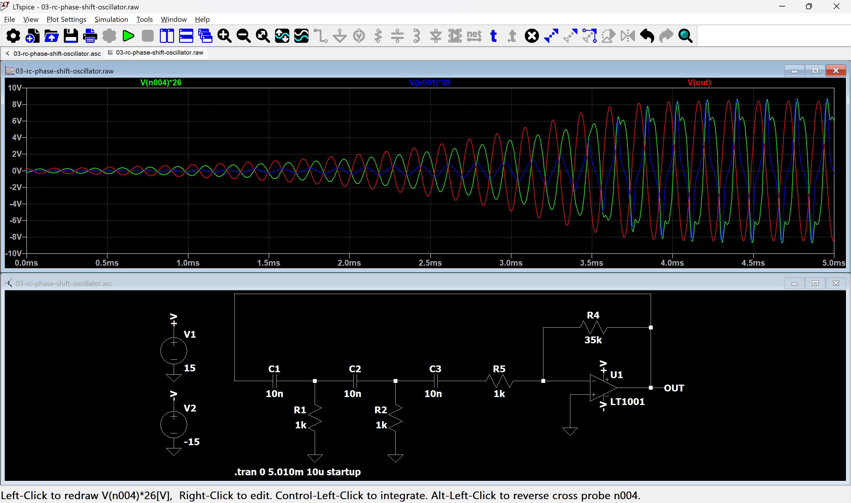
I start simulating the very first version of this circuit by Cătălina “Tank”:
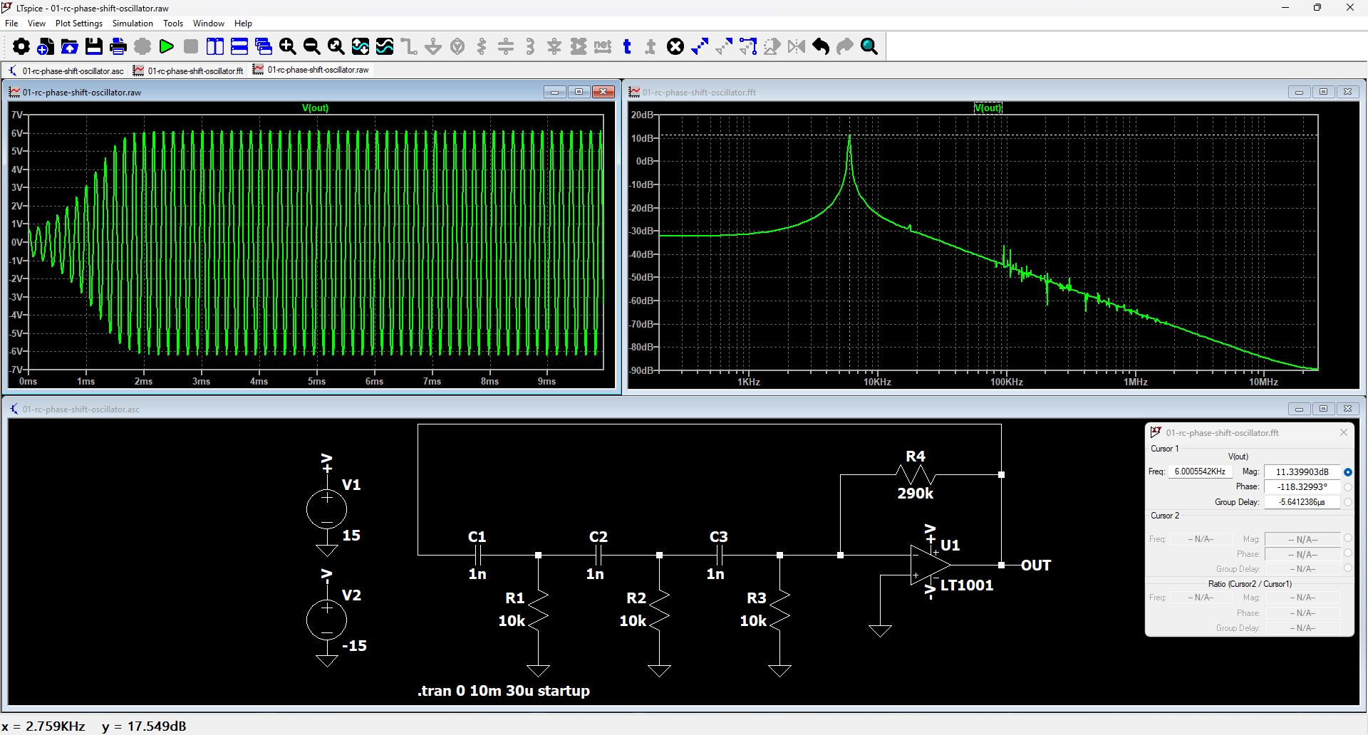
On a first glance, nothing worth a fight. Seems to be a boring oscillator.
Next I found this mail of Andreas “Bullterrier”:
“Weird circuit… First, R3 should not have any effect. Second, why your frequency is shifted from the theoretical 6.5 kHz to 6.0 kHz ?”
First point seems rather sound…
A few mails later, this mail by Cătălina “Tank”:
“You stubborn! Simulations DOES show it has an effect.”
I was thinking this is typical from Cătălina when she lacks coffee… until I ran a simulation:
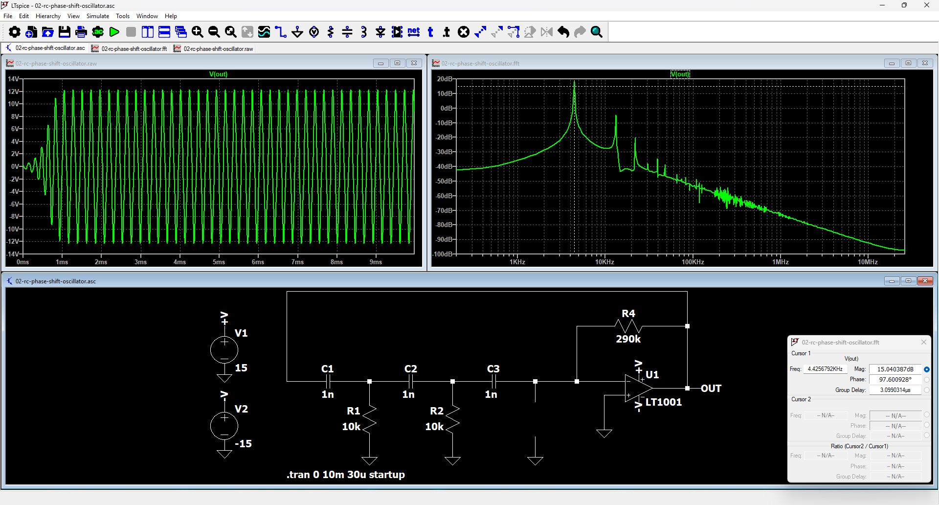
Holy damn. The resistor which should have no effect DOES HAVE an effect, and now the frequency is even further away from the theory: 4.5 kHz.
…even further
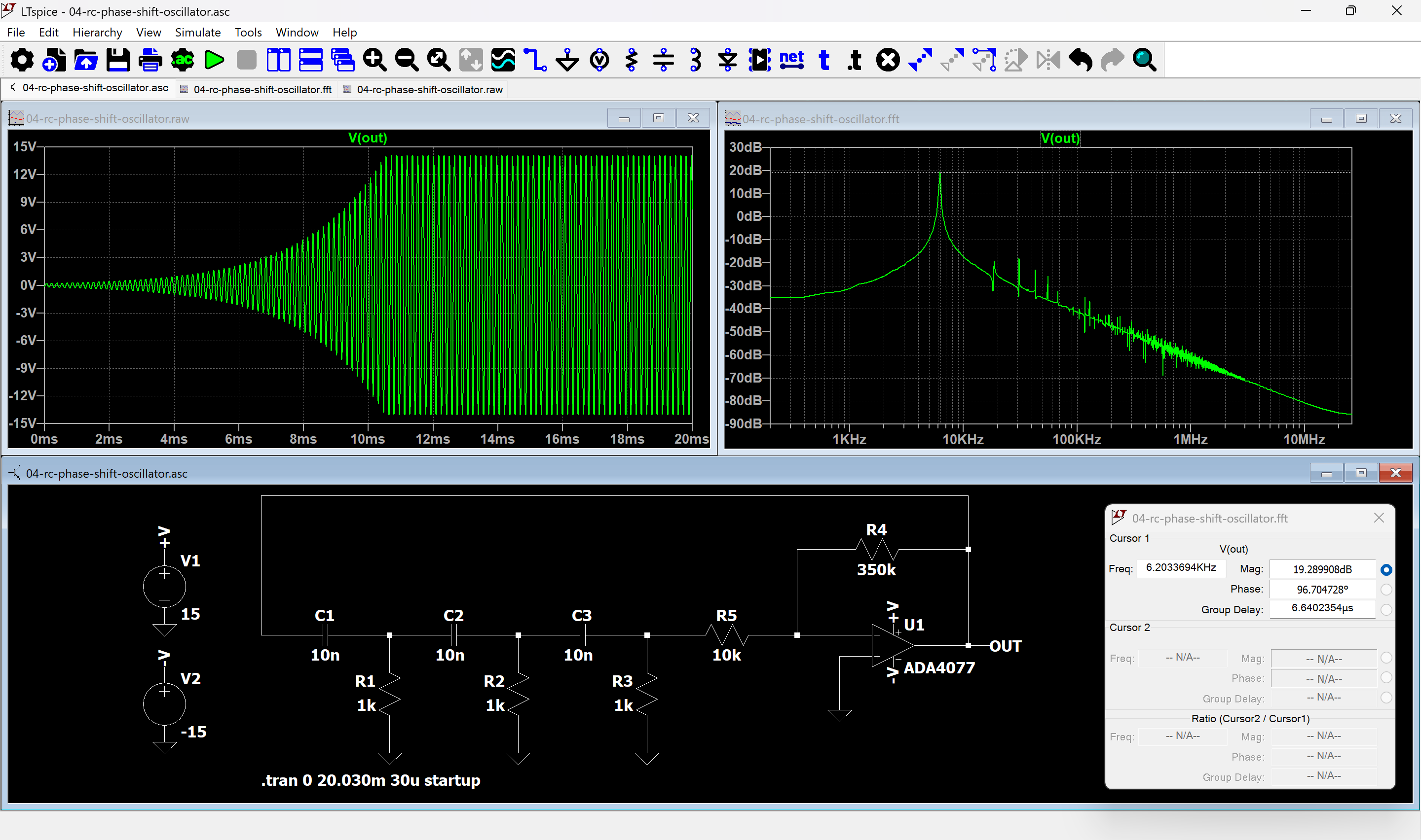
Next I simulate the first version proposed by Andreas “Bullterrier” which uses the input resistor of the inverting operational amplifier as an equivalent of the final shunt resistor:
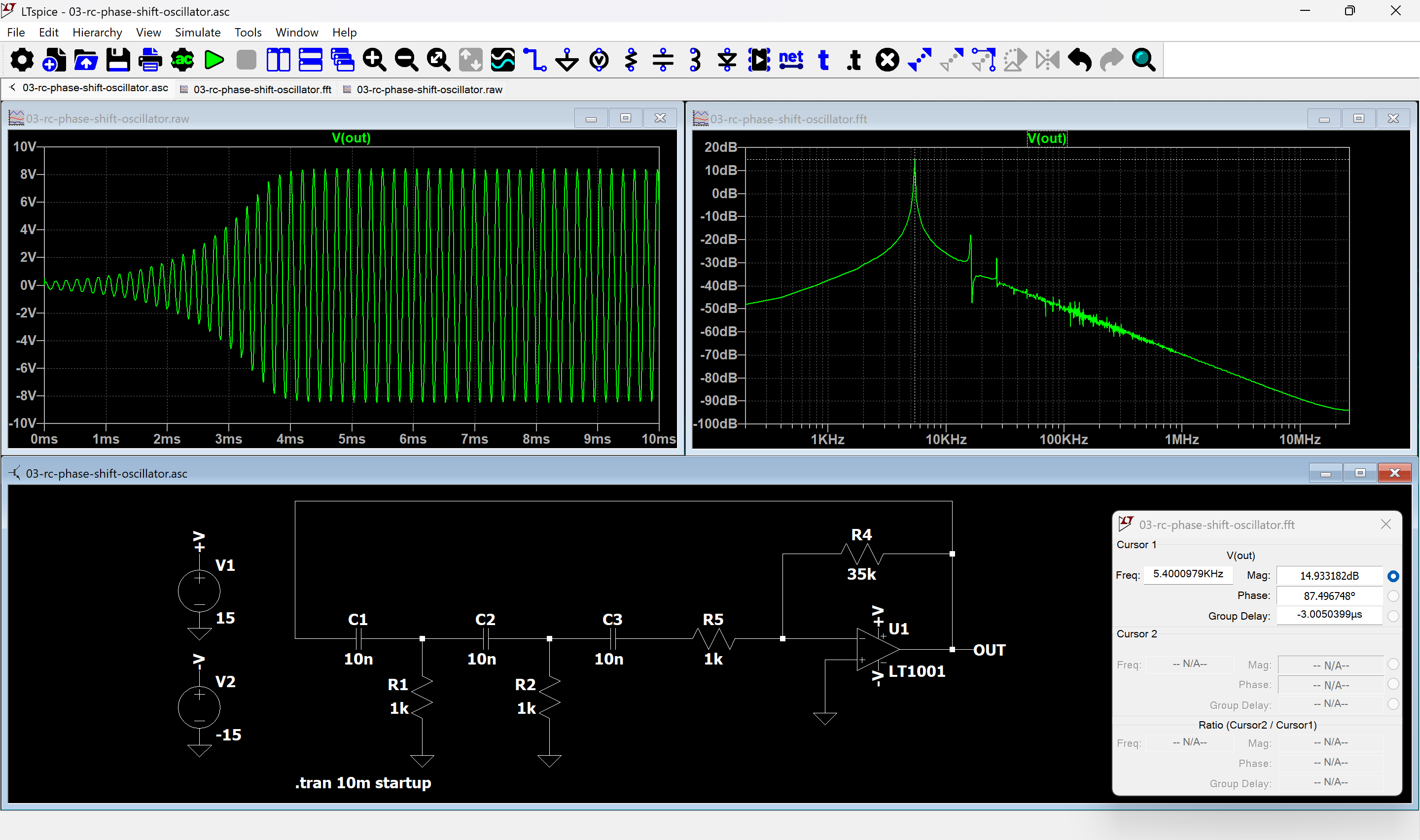
The frequency is far from the theory, 5.0 kHz instead of 6.5 kHz, and the gain needed for a quick start higher than the theory.
Digging in the problem
All this stuff semm to have one question in common: what is actually the impedance of the operational amplifier circuit, no matter its variant.
I made a Lissajous diagram to have a first look at the impedance:
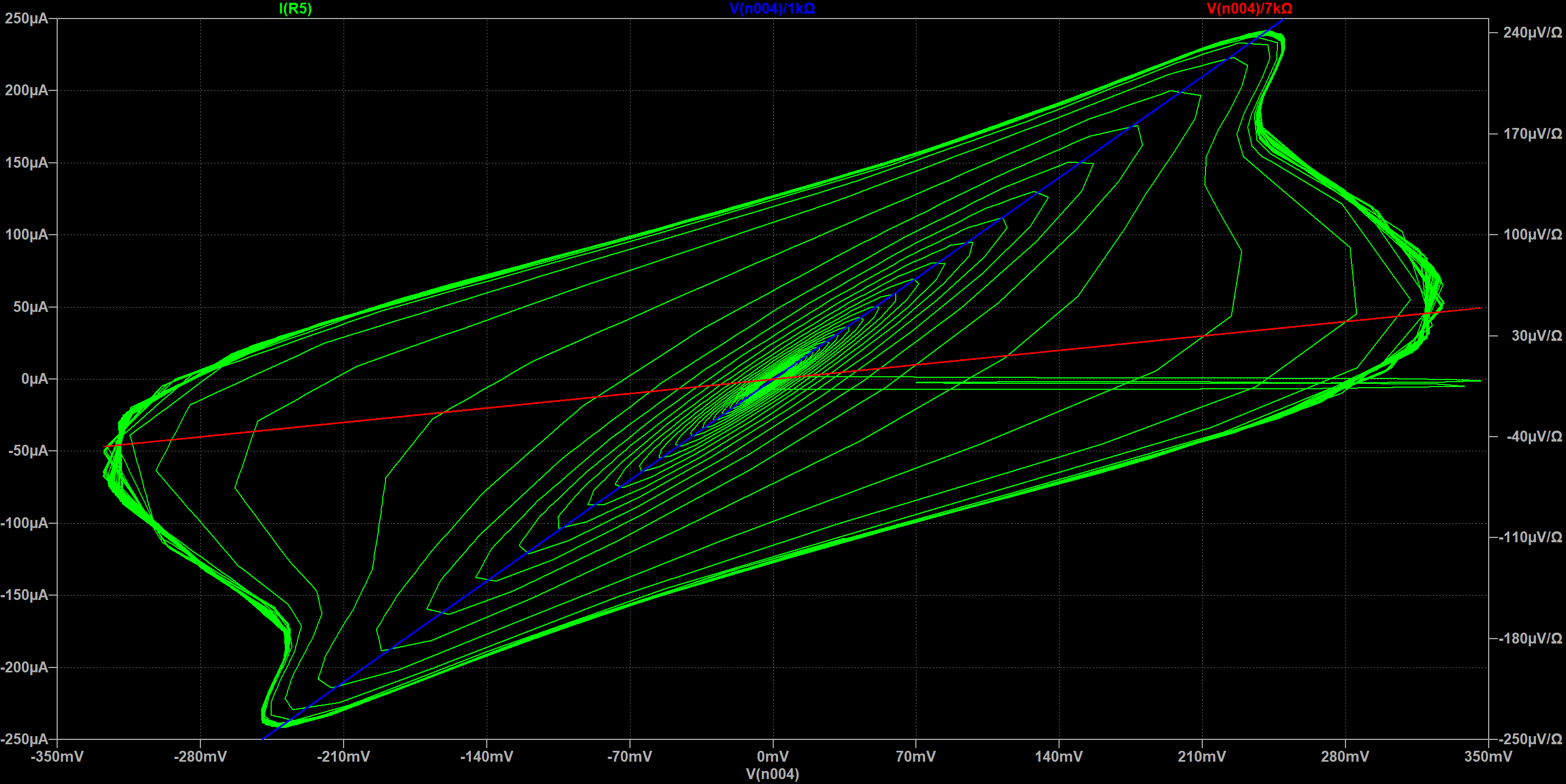
We see that for low amplitudes the trajectory (green) is close to a 1 kΩ resistance (blue) but that for higher amplitudes the trajectory becomes much more complex, with a mixture of reactive behavior and of non-linearities for an equivalent impedance around 7 kΩ, much higher than expected at a first glance.
Andreas striked back
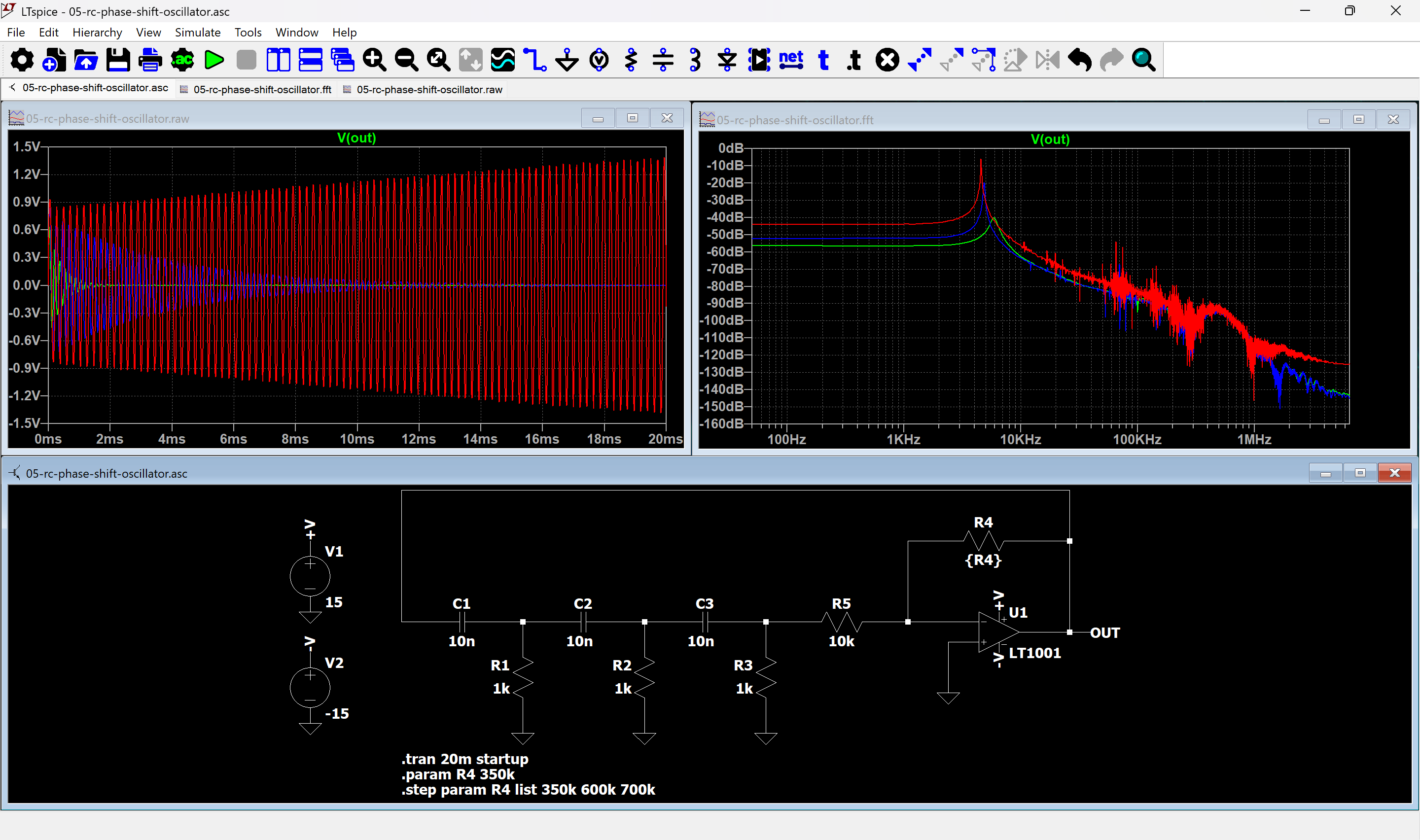
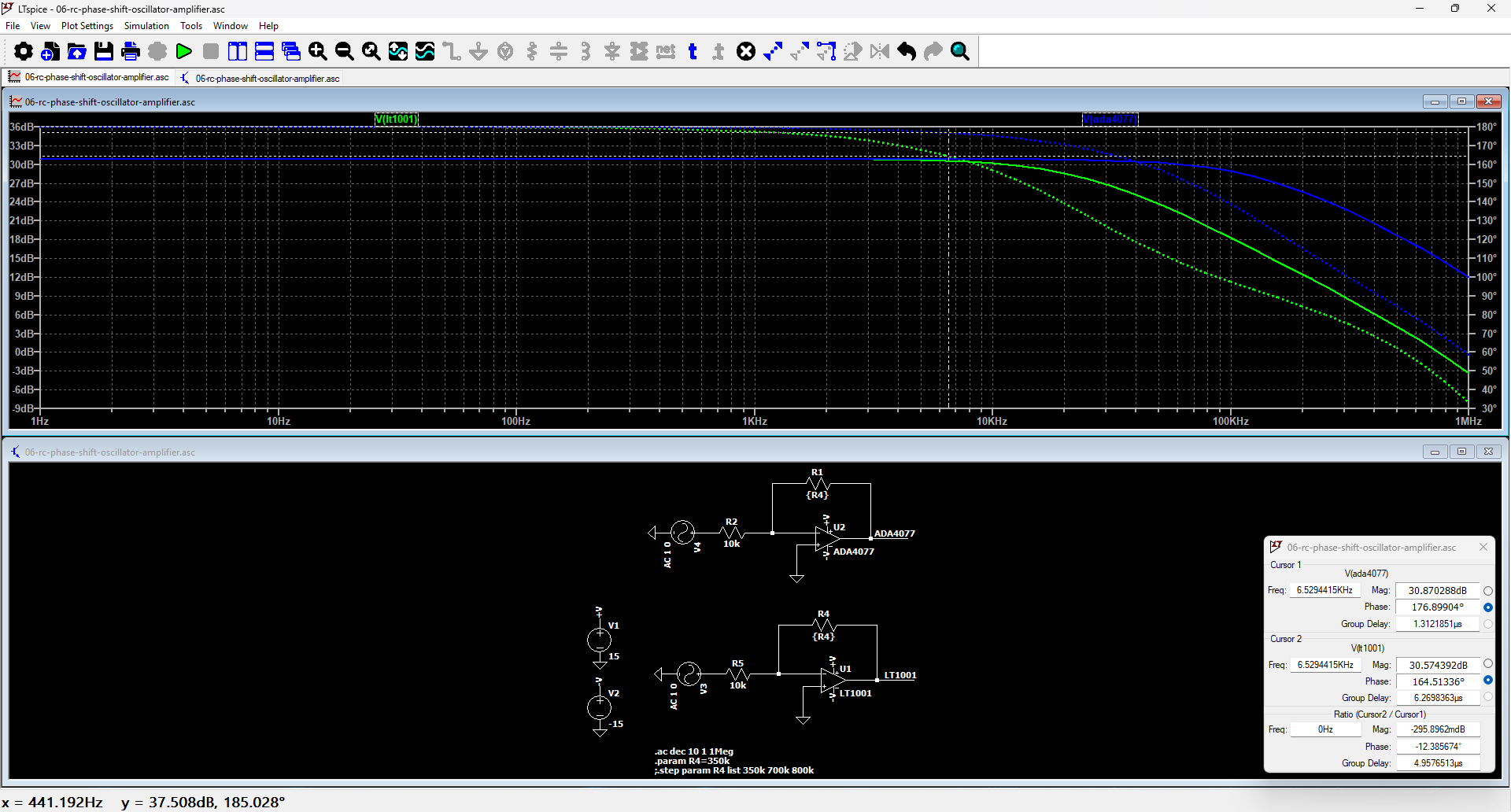
Andreas seems to have seen that the input impedance of the inverting amplifier what not the expected value since he made this second version I simulate:
Indeed he used a shunt resistor and did not rely anymore on the input impedance of the operational amplifier. The oscillation frequency, 6.2 kHz, is closer to the expected value of 6.5 kHz. Again the needed gain is higher. But seems rather fine except…
Cătălina stikes back
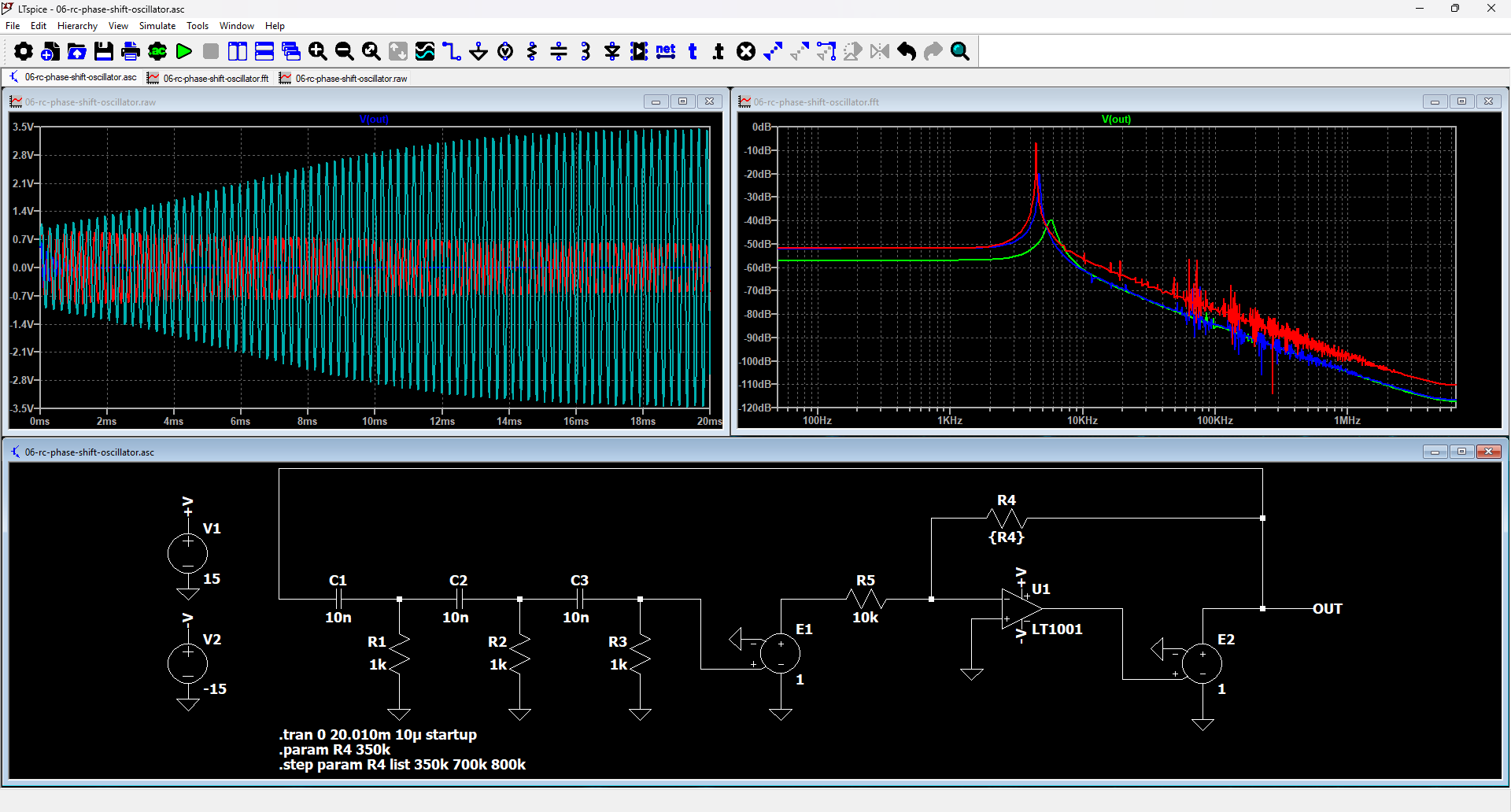
"You ******* cheater. You made a comparison between circuits but changed the operational amplifier. Your damn **** does not work with the original amplifier while my circuit does."
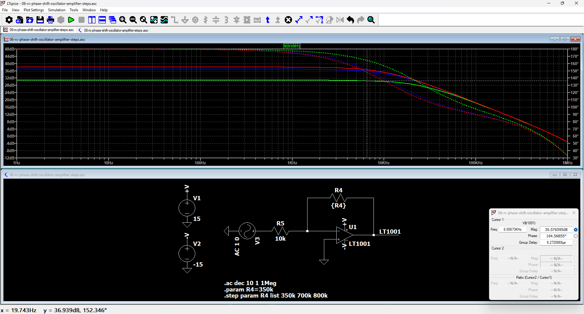
Indeed I missed this change. And when simulating with the original amplifier:
I need feedback amplifier gains much higher than the theoretical value, and the oscillation frequency, somewhere around 4.5 kHz was very far from the expected 6.5 kHz.
Digging
I tried first to check for any loading effects by introducing ideal followers before the RC and before the operational amplifier with its feedback:
Same tendencies, and the needed resistances are even worse. So, this problem is not in the impedances but really in the transfert functions. Since this problem depends on the operational amplifier, it is the point to check. And since it concerns also the low amplitude part, it should be seen also in small signal.
So I made a small signal simulation of the amplifying part with both operational amplifier models to compare:
The LT1001 has a low gain-bandwidth product, around 400 kHz in simulation, sufficient to provide the gain requested by the feedback, but with a 15.5° phase delay compared to the ideal value. On the contrary, the ADA4077 had only a 3.1° phase delay. Note the gain with both amplifiers is almost identical.
15.5° would not seem enough to wreak a circuit, but maybe RC phase shift oscillators are pricky ?
I begin to realize that this circuit might be monster and that it drove mad Andreas and Cătălina for a reason…
Next step is to simulate the RC network:
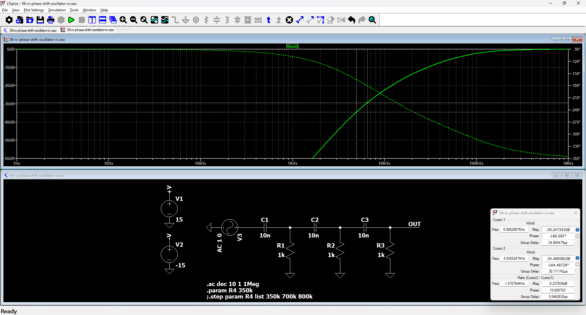
At the frequency shift needed to have a 15.5° phase advance to compensate the amplifier phase delay, a +5.2dB gain increase is needed to compensate the increased losses of the RC network. The value alone is not sufficient to explain the needed resistor values. However, when increasing the gain feedback resistor:
… the phase shift also increases, which increases again the losses of the RC network, which explains well the needed resistor values.
Straight to a solution
Enough of such falsely simple circuits. Lots of experimenters think they are simple because they manage to get something. But after how many hours of work ? And working reliably ? And at the correct frequency ? And so on. Making such oscillators is not as simple as it looks, and the story of Andreas and Cătălina is here to remind us this.
Time to enter in the 21th century.
The solution is simple and straightforward and is called direct digital synthesis (DDS):
|
|
Before detailing the subject, it is interesting to ask why using digital logic and digital to analog converters with their thoussands of integrated circuit transistors gets simpler than analog circuits with less than 20 integrated circuit transistors. The answer is in the question:
Because it leverages the specificities of integrated circuits.
The digital stuff and its thoussand of transistors can be easily integrated in integrated circuits, while the RC stuff is harder and takes lots of space. For instance, the compensation capacitor of the original 741 takes 1/3 of the chip according to Horowitz&Hill. The development is very costly, but can be reused in a much higher number of circuits than a particular RC oscillator.
Before the details, please take a break with a cat, courtesy of Wikipedia:

From a practical point of view, to use a DDS, you need:
-
A stable reference clock. But even the lowest cost crystal oscillator is better than RC oscillators. Advice: take an integrated stuff directly outputting a logic level clock. Making an oscillator from a crystal is not very hard, but don’t bring anything.
-
A DDS integrated circuit. Either bare or in a demo board which also integrates the quartz.
-
A microcontroller to set the DDS frequency. For this, use whatever you like. Also, the microcontroller is often already here.
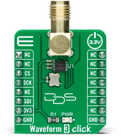
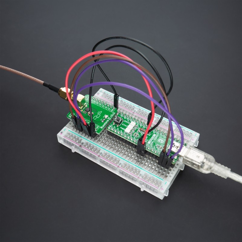
The schematic of the MIKROE waveform 3 click schematic, shown below, is self explanatory, except the dubious layout and grounding:
-
Greed LED and its resistor are mere convenience gadgets.
-
They used an integrated crystal like I advised.
-
And the DDS needs no other components than the decoupling capacitors.
However, the layout and ground split is more dubious. I would advise as first intension a single ground plane and read again the “seven habits of successful 2-layer board designers” by Eric Bogatin at https://www.signalintegrityjournal.com/blogs/12-fundamentals/post/1207-seven-habits-of-successful-2-layer-board-designers.
The schematif of the DDS itself, shown below, deserve more comments:
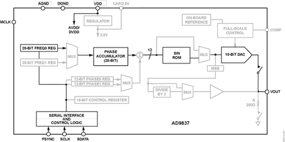
Parts not needed for understanding the base principle were lowered .
A synchronous serial interface allows to configure the chip. Particularly it allows to set the contents of a register containing the frequency. For each output sample, the phase of the output sinus is calculated by an addition. The phase accumulator overflows determine the signal period.
From this phase accumulator, an approximate sinus table is used to calculate the actual values of the samples. The two main sources of approximation are the truncature of the phase register, which determines the level of spurious, and the numbers of bits, which is the same as the ADC. After the sinus table, which converts the phase into a digital value, the digital to analog converter produces the actual voltage.
Other stuff in the schematic are:
-
A second frequency register to allow to easily commute between two frequencies.
-
A phase shift register to allow to easily commute between two phases of the signals. Note this register would not be very interesting if there were only one.
-
A control register to control the various parts (frequency and phase register selection, …).
-
A 2.5V regulator to supply the inners of the chip and to avoid the user to do this itself.
-
A bypass of the sinus table to produce ramps.
-
A circuit to directly produce a divided clock instead of a sinus.
-
A circuit to control precisely the full scale amplitude of the digital to analog converter.
Now, time to write the report and to ask for payment in liters of coffee.
Epilogue
I received as a payment for this stuff approximately 50 liters of coffee, the standard currency in use at ACME labs.
The fancy oscillator stuff was dropped and replaced by very convenient DDS synthesizers.
Andreas and Cătălina have stopped their fight and promised to never touch damn circuits.
And on my side, still have a few cats to replace by more explanations, nothing new on the sun.
Appendix
A previous version of this article included some picture of a cat instead in waiting of the explanations to come. Please find it again:
