Details of calculations for active bandpass filter with finite GBW operational amplifier.
31 Dec 2025
Many thanks to Christophe Basso to have showed me the factorisation technique which is the key of this work.
Introduction
Active operational amplifier filters, called VCVS in the jargon, are a convenient way to implement low frequency filtering, particularly when operational amplifiers are already used for amplification.
Design equations are readily available but often don't take into account the needed correction for finite GBW of the operational amplifier.
Texas Instruments SBAA236 application note provides a compensation scheme using additional components, very efficient but overkill for lots of applications.
This page presents simple equations for analysis and synthesis of VCVS filters with finite GBW operational amplifiers.
The voltage at point x, V_x, can be calculated using Millman theorem:
\begin{multline*}
V_x = \frac{
\frac{V_\text{TH}}{R_\text{TH}}+\frac{V^-}{\frac{1}{C \cdot s}}
+ \frac{V_\text{out}}{\frac{1}{C \cdot s}}
}{
\frac{1}{R_\text{TH}}
+ \frac{1}{\frac{1}{C \cdot s}}+\frac{1}{\frac{1}{C \cdot s}}
}
= \frac{
\frac{1}{R_\text{TH}} \cdot V_\text{TH}
+ C \cdot s \cdot V^-
+ C \cdot s \cdot V_\text{out}
}{
\frac{1}{R_\text{TH}}
+ 2 \cdot C \cdot s
}
\end{multline*}
The V^- voltage can be calculated in the same way:
\begin{multline*}
V^- = \frac{
\frac{V_x}{\frac{1}{C \cdot s}}
+ \frac{V_\text{out}}{R_2}
}{
\frac{1}{\frac{1}{C \cdot s}}
+ \frac{1}{R_2}
}
= \frac{
C \cdot s \cdot V_x
+ \frac{1}{R_2} \cdot V_\text{out}
}{
C \cdot s
+ \frac{1}{R_2}
}
= \frac{
R_2 \cdot C \cdot s \cdot V_x
+ V_\text{out}
}{
1 + R_2 \cdot C \cdot s
}
\end{multline*}
Combining both equations:
V^- = \frac{R_2 \cdot C \cdot s}{1 + R_2 \cdot C \cdot s} \cdot \left[
\frac{
\frac{1}{R_\text{TH}} \cdot V_\text{TH}
+ C \cdot s \cdot V^-
+ C \cdot s \cdot V_\text{out}
}{
\frac{1}{R_\text{TH}}
+ 2 \cdot C \cdot s
}
\right] + \frac{1}{1 + R_2 \cdot C \cdot s} \cdot V_\text{out}
Multiplying both sides of the equation by \left[ 1 + R_2 \cdot C \cdot s \right] \cdot \left[ \frac{1}{R_\text{TH}} + 2 \cdot C \cdot s \right]:
\left[ 1 + R_2 \cdot C \cdot s \right] \cdot \left[ \frac{1}{R_\text{TH}} + 2 \cdot C \cdot s \right] \cdot V^-
= R_2 \cdot C \cdot s \cdot \left[
\frac{1}{R_\text{TH}} \cdot V_\text{TH}
+ C \cdot s \cdot V^-
+ C \cdot s \cdot V_\text{out}
\right]
+ \left[ \frac{1}{R_\text{TH}} + 2 \cdot C \cdot s \right] \cdot V_\text{out}
Multiplying by R_\text{TH} to outline the time constant units:
\left[ 1 + R_2 \cdot C \cdot s \right] \cdot \left[ 1 + 2 \cdot R_\text{TH} \cdot C \cdot s \right] \cdot V^-
= R_2 \cdot C \cdot s \cdot \left[
V_\text{TH}
+ R_\text{TH} \cdot C \cdot s \cdot V^-
+ R_\text{TH} \cdot C \cdot s \cdot V_\text{out}
\right]
+ \left[ 1 + 2 \cdot R_\text{TH} \cdot C \cdot s \right] \cdot V_\text{out}
Developping and regrouping terms according to their voltage:
A previous version of this article presented a further first order approximation of this equation using the hypothesis \frac{2 \cdot Q}{\omega_\text{BW} \cdot \tau_0} \ll 1. This hypothesis is inaccurate in though cases, like the example to come using an LM324, and bring no additional value. Sorry for the inconvenience.
The previously done hypothesis allows to calculate the needed values of the components. However, they are not necessarily realisable, for instance when the equations give negative values. The conditions for realisability are as follows:
\omega_\text{BW} \geq \frac{Q}{\tau_0}
Which can be interpreted as the gain-bandwidth of the operational amplifier must be higher than the filter frequency multiplied by a factor depending of the quality factor Q.
Hypothesis verification
Factorosation hypothesis
Remind the hypothesis:
\tau_0^2 \gg \frac{\tau_0 \cdot \tau_p}{Q}
Equivalent to:
\frac{\tau_p}{Q \cdot \tau_0} \ll 1
It is difficult to have an exact expression for τ_p, but a bound allows to check the hypothesis:
In the project which gave me the opportunity to write this article, I simply used a 10 MHz GBW op-amp. However, to test GBW compensation equations, a lower GBW op-amp is a much better test. Indeed, it was this test which allows me to detect and fix a mistake in the previous version.
JLCPCB offers a reduced price on the PCBAs using a reduced list of components. Components from this list are listed below:
NE5532DR output 2 V to Vcc - 2 V, not convenient for 5 V operation
TL072CDT 6 V min Vcc
LM393DR2G not an op-amp but a comparator
OP07CDR 6 V min Vcc
LM358DR2G 0 V to Vcc - 2 V, half LM324
LM324DT 0 V to Vcc - 2 V
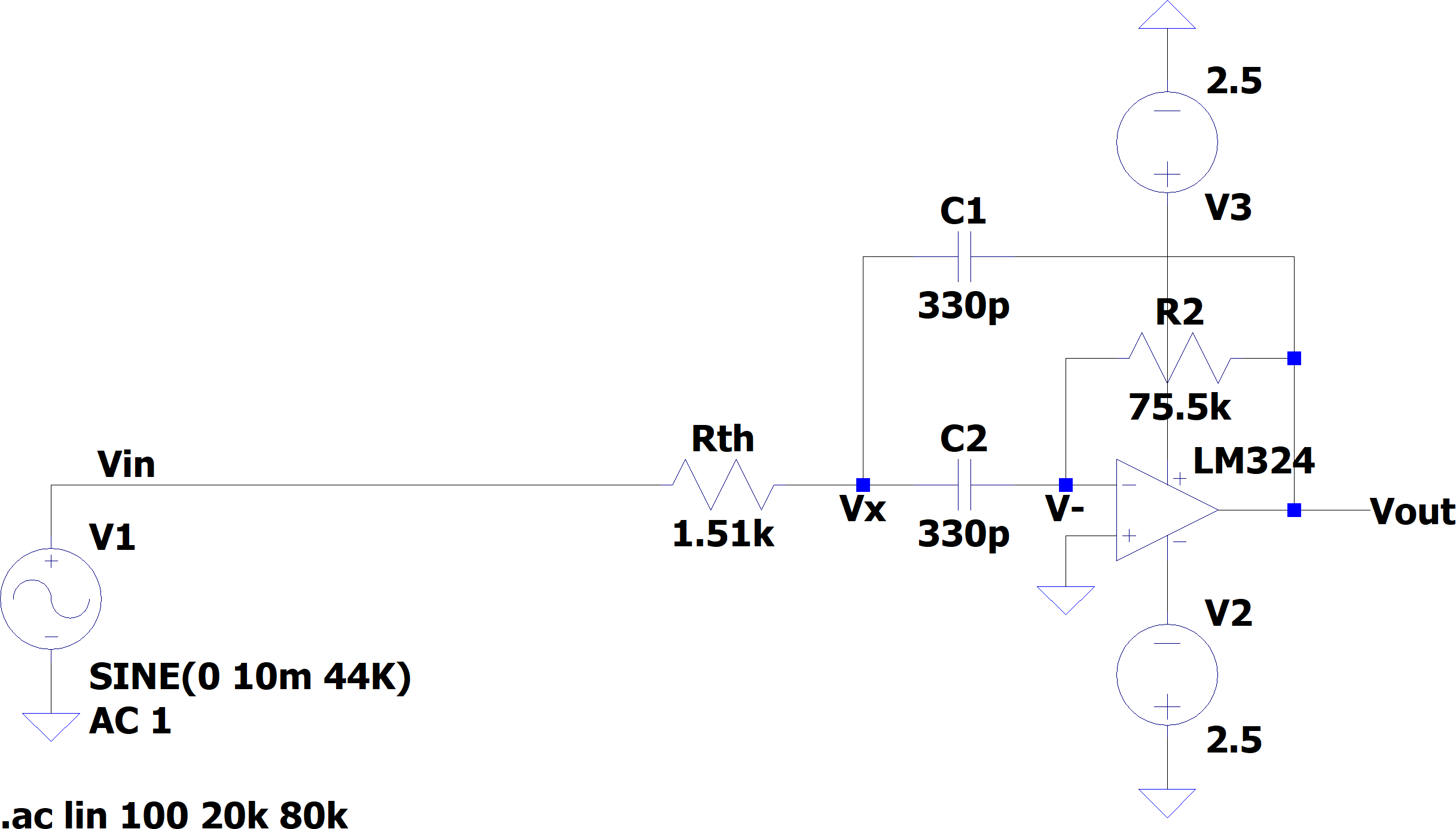
The LM324 is selected.
Different values of its GBW are present in the various datasheets, but we'll stick to the most common value of 1.2 MHz.
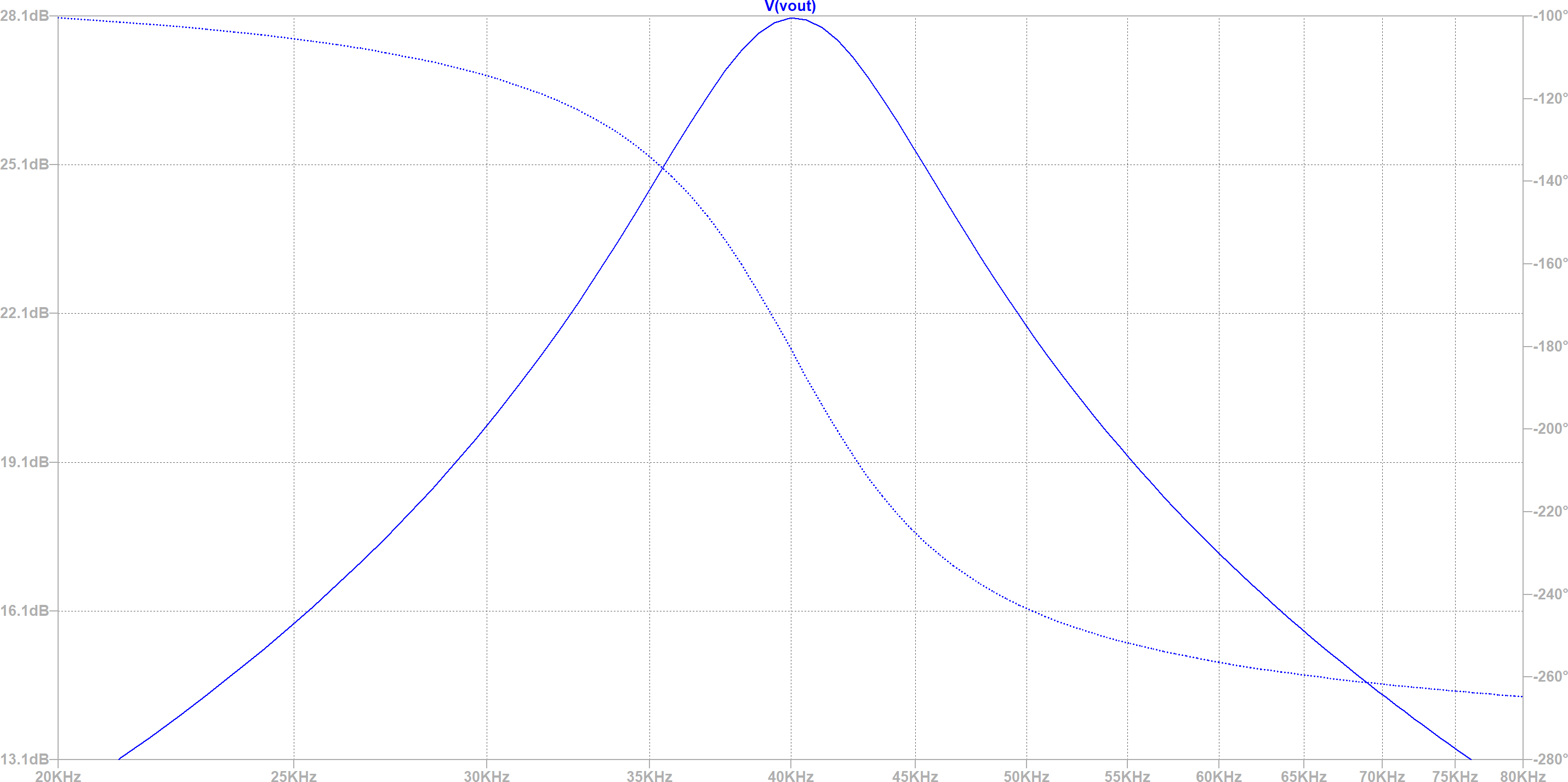
The following example filter was designed for a 40 kHz center frequency and a Q of 4 (10 kHz bandwidth). Schematic and simulation results are shown below:
 RF cat corner